
Journal of Nanoscience and Nanoengineering, Vol. 1, No. 3, October 2015 Publish Date: Aug. 17, 2015 Pages: 107-114
Empirical Ratio of First Two Optical Transition Energies in Semiconducting Single Wall Carbon Nanotubes
G. R. Ahmed Jamal1, *, S. M. Mominuzzaman2
1Department of Electrical and Electronic Engineering, University of Asia Pacific, Dhaka, Bangladesh
2Department of Electrical and Electronic Engineering, Bangaldesh University of Engineering and Technology, Dhaka, Bangladesh
Abstract
In this work, the ‘ratio problem’ between first and second optical transition energies of semiconducting single-wall carbon nanotube is discussed. Possible reasons behind the deviation of experimentally observed ratio between first two optical transitions from theoretically predicted ratio is mentioned. A number of semiconducting single-wall carbon nanotubes having chiral index (n, m) with mod (n-m, 3) ≠ 0, and having diameter in between diameter range of 0.4 nm and 3 nm are considered. First and second optical transition energies of all those tubes are recorded from various reports of optical spectroscopic experiments and recoded data was closely scrutinized. Based on that observation, ratio of first and second optical transition energies for all semiconducting tubes is expressed empirically through an empirical expression in terms of diameter, chiral index (n, m) and mod value. The empirical ratio matched very well with experimental ratio over the full diameter range. The proposed empirical way of expressing this ratio may greatly help in finding the proper ratio of first two optical transitions without depending on experimental values of two transitions. The generated pattern from the plot of this empirical ratio can also help in Photoluminescence based chirality assignment.
Keywords
Single Wall Carbon Nanotube, Optical Transition, Tight Binding Model, Ratio Problem, Chiral Index
Received: July 6, 2015
Accepted: August 3, 2015
Published online: August 17, 2015
@ 2015 The Authors. Published by American Institute of Science. This Open Access article is under the CC BY-NC license. http://creativecommons.org/licenses/by-nc/4.0/
1. Introduction
Electronic and optical properties of single-wall carbon nanotubes (SWCNT) are directly associated with their geometrical structures [1,2] which are uniquely specified by a pair of chiral index (n, m). A SWCNT (n, m) will be metallic if its n-m = 3k (k is integer), i.e. mod (n-m, 3) = 0 and it will be semiconducting if its n-m ≠ 3k, i.e. mod (n-m, 3) = 1 or 2 [3]. This relation gives two types of semiconducting SWCNTs, mod 1 type and mod 2 types.
The one-dimensionality of the Single Wall Carbon nanotubes (SWCNT) gives rise to 1D sub-bands instead of one wide electronic energy band in nanotube density of states (DOS). Each SWCNT (n, m) has a unique set of interband transition energies Eii denoting the energy differences between the i-th conduction and valence bands and optical transitions can only occur between these mirror sub-bands [1,2,4,6].
The tight-binding (TB) model of π-bands of graphene using the zone-folding approximation has been widely used for modeling electronic band structure of single-wall carbon nanotube (SWCNT) due to its simplicity, low computational cost, and qualitative agreement with experimental results [7-9]. TB model with the nearest-neighbor approximation provides following simple expression to calculate optical transitions of a SWCNT [1,2,10]:
![]() (1)
(1)
Where, ![]() is the nearest-neighbor hopping parameter,
is the nearest-neighbor hopping parameter, ![]() Å is carbon-carbon bond length,
Å is carbon-carbon bond length, ![]() is nanotube diameter in nm, given by
is nanotube diameter in nm, given by ![]() and j is an integer. Eii corresponds to the first, second, third, fourth… interband transitions (E11S, E22S, E33S, E44S….) of semiconducting SWCNT when j = 1, 2, 4, 5… respectively. This inverse proportional trend of transition energies with SWCNT diameter, given by Eqn. (1), is also observed from the Kataura plot [11,12] and from other optical spectroscopic experiments [6,13].
and j is an integer. Eii corresponds to the first, second, third, fourth… interband transitions (E11S, E22S, E33S, E44S….) of semiconducting SWCNT when j = 1, 2, 4, 5… respectively. This inverse proportional trend of transition energies with SWCNT diameter, given by Eqn. (1), is also observed from the Kataura plot [11,12] and from other optical spectroscopic experiments [6,13].
Here, the first optical transition (E11) is the bandgap of semiconducting SWCNTs and the second optical transition (E22) facilitates various optical spectroscopic experiments, as it falls within visible energy range. Also, for photo absorption in SWCNTs, first two optical transitions are mainly considered. Hence, E11 and E22 of semiconducting SWCNTs are more significant than other transitions and are of more interest [14].
Basic tight binding model has a number of limitations due to which Eqn (1) cannot give complete description of different optical transition energies in SWCNTs. These limitations are attributed to many factors. One major factor is nanotube ‘curvature effect’ induced band structure deviation from simple π-orbital graphene picture [11-14]. Other factors are ‘chirality effect’ [15], ‘trigonal warping effect’ [9,11,16] and many body effect (electron-electron interaction) comprising self-energy and exitonic effect [17-22]. One effect of such limitation is basic TB model predicts inaccurate ratio of first two optical transitions [14].
2. The ‘Ratio Problem’
It has been observed from some optical spectroscopic experiments that basic TB model fails to explain experimentally observed ratio of first two optical transition energies of semiconducting SWCNTs (E22S/E11S). Nearest neighbour TB model and the corresponding Eqn (1) predicted this ratio to be 2. Extended TB model later predicted that this ratio will be lesser than 2 at small diameters but will approach 2 asymptotically for large diameters [21]. In practice, experimentally observed ratio was found to oscillate below and above 2 (down to 1.17 and up to 2.6) for different chiralities and converge to only around 1.8 for large diameters [21-26]. This problem is often referred as ‘ratio problem’ in literatures [21]. Neither the simple TB model nor the extended TB model could account this observation fully.
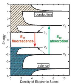
Figure 1. Schematic density of electronic states for a single nanotube structure. Solid arrows depict the optical excitation and emission transitions of interest; dashed arrows denote non-radiative relaxation of the electron (in the conduction band) and hole (in the valence band) before emission. Figure is taken from [14].
2.1. Experimental Reports on Ratio Problem
In 2002, Bachilo et al [14] and O’ Connel et al [27] independently performed two very important fluorescence spectroscopy experiments and observed band gap luminescence from SWCNTs for the first time. As shown in Fig 1, light absorption at photon energy E22 is followed by fluorescence emission near E11. The values of E11 and E22 will vary with tube structure. Bachilo et al [14] observed that absorption (E22) and emission (E11) energies from SWCNTs differ from theoretical predictions of tight binding calculations. Their measured optical transition frequencies (υii) deviate from simple diameter dependence more strongly than expected. For example, they found υ22 value of the (9,2) tube is 26% higher (by 3700 cm-1 or 0.46 eV) than that of (9,1), even though its diameter is only 6% larger. In addition, as tube diameter increases, they found the υ22/ υ11 (or, E22/E11) ratio apparently approaches a value around 1.75, smaller than tight binding prediction, thus causing ‘ratio problem’. Their excitation versus emission frequency plot showed a blue shift of these frequencies though they did not highlight this observation in their report.
Sfeir et al [13] observed from their Rayleigh scattering experiment that the mod 1 type semiconducting SWCNT have smaller transition energies than mod 2 type for odd transitions (E11S, E33S,….) whereas, mod 2 type semiconducting SWCNT have smaller transition energies than mod 1 type for even transitions (E22S, E44S,….) with comparable diameters. This observation is not reflected by Eqn (1) as it gives comparable values of transition energies for comparable diameters with any constant![]() , irrespective of mod type. This observation also says that E22/E11 ratio for mod 1 and mod 2 type semiconducting SWCNTs will follow slightly different trend. Thus, with increasing diameters of SWCNTS, the E22/E11 ratio will not be uniformly decreasing, rather will rise and fall continuously with the change of mod value.
, irrespective of mod type. This observation also says that E22/E11 ratio for mod 1 and mod 2 type semiconducting SWCNTs will follow slightly different trend. Thus, with increasing diameters of SWCNTS, the E22/E11 ratio will not be uniformly decreasing, rather will rise and fall continuously with the change of mod value.
Kane et al [21] and Mele et al [22] reported ‘blue shift’ of transition energies which is also not reflected through Eqn (1). They observed this problem after scrutinizing fluorescence spectroscopy results reported by Bachilo et al [14] and O’ Connel et al [27]. They plotted observed optical energies of SWCNTs measured in fluorescence spectroscopy as a function of n/3R and showed that E11 and E22 deviate from simple linearized tight binding model and are blue shifted by a nonlinear 1/R scaling as shown in Fig 2. They termed this observation as ‘blue shift problem’ [13,22,26].
Zhao et al [25] discussed both the ‘ratio problem’ and the ‘blue shift problem’. As per their analysis, the ratio problem is a simple consequence of nearly equal blueshifts of the two lowest optical absorptions (E11 and E22) from TB frequencies.
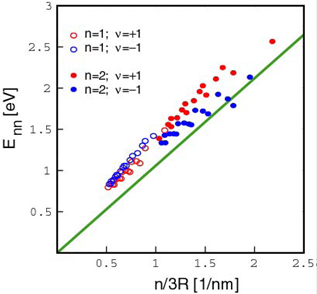
Figure 2. Observed ‘blue shift’ of optical transition energies measured from fluorescence spectroscopy, for mod 1 type (ν =+1) and mod 2 type (ν = -1) semiconducting SWCNTs. The solid line gives the prediction of linearized TB model theory. Figure is taken from [22].
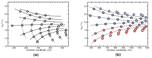
Figure 3. Comparison of fluorescence spectroscopy result with Tight Binding (TB) calculation. (a) Measured ratios of excitation to emission frequencies by Bachilo et al [14]. (b) Calculated ratio from an extended TB model for mod 1 type (blue) and mod 2 type (red). Solid lines connect families with equal n – m values and dotted line connects 2n+m families. Bachilo et al. used the correspondence between (a) and (b) for chirality assignment of each tube. It can be observed that, for large diameters, lines converge to near 1.75 in (a) and near 2 in (b). Figure is taken from [14].
2.2. Possible Causes Behind Ratio Problem
One of the reasons behind deviation of simple tight binding model from experimental results is many body effect (electron-electron interaction) [21-26,28,32]. The many body effect comprises an exciton binding energy and a self-energy. Kane et al [21], Mele et al [22], Lin et al [23], Spataru et al [24,32], Zhao et al [25], Dukovic et al [26], Samsonidze et al [33], Jiang et al [28], Sato et al [29], Ando et al [30], and Pedersen et al [31] studied the many body effect on electronic properties of SWCNTs. It is believed by some authors that the main explanation for the ‘ratio problem’ and ‘blue shift problem’ can be given by showing the effect of many body interaction in SWCNTs [21-23,25,26], even if the relative contributions of self-energy and excitonic effects are not precisely known yet. The nature and amount of many body effects are still being discussed in literatures and also much disputed. Theories which include many particle interactions are still quite rare and involve complex calculations. Therefore no complete Kataura plot has been provided so far which includes curvature effects, electron-electron and electron-hole interaction. [34].
However, a recent study of Sato et al [29] showed that, for E11 and E22 transitions, the chirality dependence of the exciton binding energy for each (n,m) SWCNT is almost cancelled by that of the self energy, both effects being of the same order of magnitude, in the range of 0.5 to 1 eV [23]. Thus the origin of the family pattern for E11 and E22 can be understood by the chirality dependence of the single particle energies, by safely ignoring many body effect.
2.3. Significance of Knowing Proper E22/E11Ratio
As the electronic and the optical properties of single wall carbon nanotubes (SWCNT) are directly related with their chirality, the determination of the chirality (n, m) of SWCNTs is a necessity before most of the applications in device level [35,36]. Identification of spectroscopic features and correlating them with nanotube geometric structure is also required to purify, identify, separate and sort nanotubes after their synthesis [37].
Photoluminescence (PL) excitation [14,38,39,43] has been one of the mainstream tools for nondestructive chirality characterization of semiconducting SWCNTs. Photoluminescence (PL) method uses optical absorption and emission energies for unique chirality assignmen [44,45].
Bachilo et al. [14] showed Photoluminescence (PL) based effective (n, m) assignment based on pattern recognition between experimental and theoretical (derived from extended tight binding model) plot of the second transition (excitation energy) versus the first transition (emission energy). A family is observed in experimental E22/E11 plot where nanotubes having same (n-m) values fall along same symmetric lines or family branches [14]. These families are directly linked with their chiral index values.
In their method of chirality assignment, after measuring optical excitation and emission energies they plotted the ratio of excitation to emission energies for each peak versus the peak’s excitation wavelength. The result is shown in Fig. 3(a). The pattern of solid lines through these experimental points qualitatively resembles the pattern shown in Fig. 3(b), which displays computed findings from an extended tight-binding model calculation on SWCNTs. Lines have been drawn through points of species that share the same value of n – m, referred as nanotube families. The analogy between the simulation of Fig. 3(b) and the experimental pattern of Fig. 3(a) enables them to sort the observed data points into families marked by the solid lines in Fig. 3(a). Their method established Photoluminescence based chirality assignment of semiconducting SWCNT as an effective method for unique assignment using E22/E11 ratio plot.
3. Proposed Empirical Formula to Predict Proper E22/E11 Ratio
As discussed earlier, theoretical formulation of ‘ratio problem’ is not completed yet as its causes are still under discussion. So, an empirical formula may fill that gap and will be much useful to predict this ratio correctly. If an empirical ratio plot can be generated from an empirical expression of E22/E11 ratio that matches very closely with known experimental data, then unknown chiral index can be easily found if experimental ratio plot is superimposed on the empirical ratio plot.
In this work, a large number of SWCNTs having diameter ~0.4 nm to ~3 nm are considered. Using the condition mod (n-m, 3) = 1 or 2 for semiconducting SWCNTS, we found total 212 semiconducting SWCNTs within this diameter range, comprising both zigzag and chiral tubes. After dividing them according to their mod value we found 110 mod 1 type and 102 mod 2 type semiconducting SWCNTs. Chiral index of these semiconducting SWCNTs, within this diameter range, starts from (4, 2) tube with diameter 0.42 nm) and extends up to (23, 22) tube with diameter 3.094 nm. After sorting them according to their mod value, we found 110 mod 1 type and 102 mod 2 type semiconducting SWCNTs.
Values of first and second optical transition energies (eV) corresponding to all these semiconducting SWCNTs are recorded from various reports of different optical spectroscopic experiments [6,10,12,14,27,44,46,47,38,48,63]. Recorded data showed that E11 for mod 2 types are higher than that of mod 1 type whereas E22 for mod 2 types are lower than that of mod 1 type with comparable diameters. Sfeir et al [13] also reported this same observation as mentioned earlier. In order to reflect this phenomenon, it will be suitable to include a mod value related term in the proposed empirical formula so as to follow the ratio trend with the change of mod value.
Also, nanotube’s curvature (which can be represented by dt) and chirality (n, m) have direct effect on the optical transition energy values E11 and E22 which in turn has effect on E22/E11 ratio. So, the proposed empirical formula should include dt and chiral index term to reflect the effect of curvature and chirality on E22/E11 ratio. The required empirical formula should have the capacity to predict the E22/E11 ratio of SWCNT with any chirality through one single expression for both mod types without any need for calculating E11 and E22 separately. Here we have devised such an empirical formula in terms of diameter dt, chiral index ( n, m), mod value (k) and numerical fitting parameters as below:
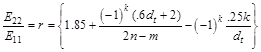 (2)
(2)
Where k= 1 or 2 for mod 1 or mod 2 type. This expression is able to give appropriate E22 to E11 ratio (r) for any semiconducting SWCNTs.
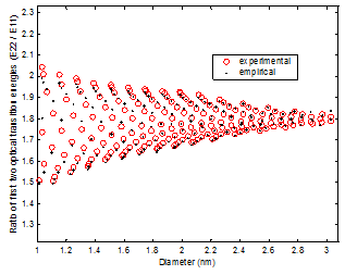
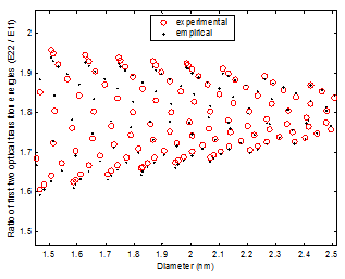
Figure 4 shows the plot of experimental and empirical E22 to E11 ratio with respect to diameter dt. The pattern similarity between Fig 4 and Fig 3 is noticeable. It can be observed from the figure that our empirically generated ratios follow experimental ratios very closely for each SWCNT. Another important observation is the ratio approaches to around 1.8 at higher diameters, which also comply with experimentally observed ratio.
(a)
(b)
Figure 4. (a) Plot of experimental E22 to E11 ratio with empirical ratio from Eqn (2) vs dt. b) An enlarged portion of the plot in (a).
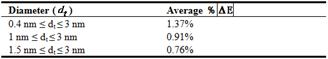
Table I gives a summary of the result. It can be noticed from Table-I that the average absolute error is less than 1% for diameter above 1 nm.
If experimental ratio plot is superimposed on this empirical ratio plot generated from Eqn (2), then unknown chiral index can be easily found. This will simplify the Photoluminescence (PL) based (n, m) assignment technique mentioned earlier as now the chirality of each tube can be readily known from the superimposed plots without the need of pattern recognition or one to one correspondence between theoretical and experimental plots.
Table I. Comparison between experimental ratio of E22 to E11 with empirical ratio from Eqn (2) and corresponding average error and % average error.
4. Conclusion
The one-dimensionality of the Single Wall Carbon nanotubes (SWCNT) gives rise to 1D sub-bands in nanotube density of states (DOS). Each SWCNT (n, m) has a unique set of interband transition energies Eii. From these transitions, first and second optical transitions, E11 and E22 of semiconducting SWCNTs, are more significant than other transitions and are of more interest. E22/E11 ratio places an important role inPhotoluminescence (PL) based effective (n, m) assignment based on pattern recognition between experimental and theoretical plot of the second transition (excitation energy) versus the first transition (emission energy). It has been observed from some optical spectroscopic experiments that basic TB model fails to explain experimentally observed ratio of first two optical transition energies of semiconducting SWCNTs (E22/E11). Basic TB model predicted this to be 2 whereas experientially found ratio is around 1.8. As proper ratio of E22/E11 is necessary for chirality assignment, so, in this work, we have proposed an effective empirical expression to get the proper E22/E11 ratio for semiconducting SWCNT with any chirality. In our proposed empirical expression the nanotube diameter dt, chiral index (n, m) and mod values are included so as to incorporate curvature effect, chirality effect and mod type effect on E22/E11 ratio. The proposed empirical relation is used to generate the empirical ratio which is compared with experimental ratio of 212 semiconducting SWCNTs. The empirical ratio was found to match very closely with experimental ratio over the full diameter range and also found to be approaching 1.8 at higher diameters like the experimental ratio. The %average deviation of empirical result from experimental result is lesser than 1% for diameter above 1 nm. This empirical ratio can simplify Photoluminescence (PL) based chirality (n, m) assignment technique to find the chiral index (n, m) of any unknown semiconducting SWCNTs.
References
- V. N. Popov, "Carbon nanotubes: properties and application", Materials Science and Engineering R, 43, pp. 61–102, 2004.
- T. W. Odom, J. L. Huang, P. Kim, and C. M. Lieber, "Structure and Electronic Properties of Carbon Nanotubes",J. Phys. Chem. B,104,pp.2794-2809, 2000.
- N. Hamada, S. Sawada, and A. Oshiyama, "New one-dimensional conductors: graphitic microtubules," Phys. Rev. Lett., Vol.68,No.10,pp.1579-1581, 1992.
- J. W. Mintmire and C. T. White, "Universal density of states for carbon nanotubes", Phys. Rev. Lett., Vol. 81, No.12, 1998.
- S. Reich and C. Thomsen, "Chirality dependence of the density-of-states singularities in carbon nanotubes", Phys. Rev. B, Vol 62, No. 7, 2000.
- M.S. Dresselhausa, G. Dresselhausc, A. Jorio, A.G. Souza Filho, R. Saito, "Raman spectroscopy on isolated single wall carbon nanotubes", Carbon, 40, pp.2043–2061, 2002.
- J. D. Correa, A. J. R. da Silva, and M. Pacheco, "Tight-binding model for carbon nanotubes from ab initio calculations," J. Phys.: Condens. Matter, Vol.22,No.7, 275503, 2010.
- R. Kundu, "Tight binding parameters for graphene", Modern Physics Letters B, Vol. 25, No. 3, pp.163-173, 2011.
- S. Reich, J. Maultzsch, and C. Thomsen, "Tight-binding description of graphene," Phys. Rev. B, Vol.66,No.3,pp.035412, 2002.
- Y. Lian, Y. Maeda, T. Wakahara, T. Akasaka, S. Kazaoui, N. Minami, N. Choi and H. Tokumoto, "Assignment of the Fine Structure in the Optical Absorption Spectra of Soluble Single-Walled Carbon Nanotubes", J. Phys. Chem. B, 107, 12082-12087, 2003.
- H. Kataura, Y. Kumazawa, Y. Maniwa, I. Umezu, S. Suzuki, Y. Ohtsuka, and Y.Achiba, "Optical properties of single-wall carbon nanotubes," Synthetic Met., Vol.103,pp.2555, 1999.
- R. B. Weisman and S. M. Bachilo, "Dependence of optical transition energies on structure for single-walled carbon nanotubes in aqueous suspension: an empirical kataura plot," Nano Lett., Vol.3,No.9,pp.1235-1238, 2003.
- M. Y Sfeir., T.Beetz, F Wang, L.Huang, X. M. H Huang., M.Huang, J. Hone, S. O’Brien, J. A Misewich, T. F.Heinz, L.Wu, Y.Zhu, L. E. Brus, "Optical Spectroscopy of Individual Single-Walled Carbon Nanotubes of Defined Chiral Structure", Science, Vol. 312, April 2006.
- Bachilo S. M., Strano M. S., Kittrell C., Hauge R. H., Smalley R. E., Weisman R. B., "Structure-Assigned Optical Spectra of Single-Walled Carbon Nanotubes", Science, Vol 298 No. 5602, pp.2361, 2002.
- V. Zólyomi and J. Kürti, "First-principles calculations for the electronic band structures of small diameter single-wall carbon nanotubes", Phys. Rev. B 70, 085403, 2004.
- V. N. Popov,"Curvature effects on the structural, electronic and optical properties of isolated single-walled carbon nanotubes within a symmetry-adapted non-orthogonal tight-binding model", New Journal of Physics, Vol. 6,2004.
- H. Zeng, H. F. Hu, J. W. Wei, Z. Y. Wang, L. Wang, and P. Peng, "Curvature effects on electronic properties of small radius nanotube," Appl. Phys. Lett., Vol.91,No.3,pp.033102, 2007.
- O. Gulseren, T. Yildirim and S. Ciraci,"A systematic ab-initio study of curvature effects in carbon nanotubes", Phys. Rev. B 65, 153405, 2002.
- J W Ding, X H Yan, J X Cao, "Analytical relation of band gaps to both chirality and diameter of single-wall carbon nanotubes", Phys. Rev. B , Vol. 66, Issue 7, Pages: 2-5, 2002.
- R. Saito, G. Dresselhaus, and M. S. Dresselhaus, "Trigonal warping effect of carbon nanotubes," Phys. Rev. B, Vol.61,No.4,pp.2981-2990, 2000.
- Kane C. L. and Mele E. J., "The Ratio Problem in Single Carbon Nanotube Fluorescence Spectroscopy", Phys. Rev. Lett. 90, 207401, 2003.
- E. J. Mele, C.L. Kane, "Many body effects in carbon nanotube fluorescence spectroscopy", Solid State Communications 135, pp. 527–531, 2005.
- H. Lin, J. Lagoute, V. Repain, C. Chacon, Y. Girard, J.-S. Lauret, F. Ducastelle, A. Loiseau S. Rousset , "Many-body effects in electronic bandgaps of carbon nanotubes measured by scanning tunnelling spectroscopy", Nature Materials 9, 235–238, 2010.
- C. D. Spataru, S. I. Beigi, L. X. Benedict and S. G. Louie, "Excitonic Effects and Optical Spectra of Single-Walled Carbon Nanotubes", AIP Conf. Proc., vol 772, p. 1061-1062, 2004.
- H. Zhao, S. Mazumdar, "Excitons in semiconducting single-walled carbon nanotubes", Synthetic Metals, 155, p.250–253, 2005.
- G. Dukovic, F. Wang, D. Song, M. Y. Sfeir, T. F. Heinz, and L. E. Brus, "Structural dependence of excitonic optical transitions and band-gap energies in carbon nanotubes," Nano Lett., Vol.5,No.11,pp.2314-2318, 2005.
- M.J. O'Connell, S.M. Bachilo, C.B. Huffman, V.C. Moore, M.S. Strano, E.H. Haroz, K.L. Rialon, P.J. Boul, W.H. Noon, C. Kittrell, J. Ma, R.H. Hauge, R.B. Weisman, and R.E. Smalley, "Band Gap Fluorescence from Individual Single-Walled Carbon Nanotubes", Science 297, pp.5581-5593, 2002.
- J. Jiang, R. Saito, Ge. G. Samsonidze, A. Jorio, S. G. Chou, G. Dresselhaus and M. S. Dresselhaus, "Chirality dependence of exciton effects in single-wall carbon nanotubes: Tight-binding model", Phys. Rev. B 75, 035407, 2007.
- K. SatoaR. Saito,J. Jiang, G. Dresselhaus, M.S. Dresselhaus, "Chirality dependence of many body effects of single wall carbon nanotubes", Vibrational Spectroscopy:Elsevier,Vol. 45, Issue 2, pp.89–94, 2007.
- T. Ando, "Family Effects on Excitons in Semiconducting Carbon Nanotubes" Journal of the Physical Society of Japan, Vol. 78, No. 10, 104703, 2009.
- T. G. Pedersen, "Exciton effects in carbon nanotubes", Carbon 42, pp.1007–1010, 2004.
- C. D. Spataru,S. I. Beigi,R. B. Capaz,and S. G. Louie, "Theory and ab initio calculation of radiative lifetime of excitons in semiconducting carbon nanotubes",Phys. Rev. Lett.,vol. 95, Issue 24, 247402, 2005.
- Ge. G. Samsonidze, R. Saito, N. Kobayashi, A. Grüneis, J. Jiang, A. Jorio, S. G. Chou, G. Dresselhaus and M. S. Dresselhaus, "Family behavior of the optical transition energies in single-wall carbon nanotubes of smaller diameters, Appl. Phys. Lett., Vol 85, No. 23, 2004.
- H. Telg, "Raman studies on individual nanotubes and nanotube ensembles –vibrational properties and scattering efficiencies", Ph.d thesis, Physics, Institute für Festkörperphysik,Berlin, 2009.
- Y. Lim , K. Yee , J. Kim , E. H. Hároz , J. Shaver , J. Kono , S. K. Doorn , R. H. Hauge , R. E. Smalley, "Chirality Assignment of Micelle-Suspended Single-Walled Carbon Nanotubes Using Coherent Phonon Oscillations", Journal of the Korean Physical Society, Vol. 51, No. 1, pp. 306-311, 2007.
- C. Thomsen, H. Telg, J. Maultzsch and S. Reich, "Chirality assignments in carbon nanotubes based on resonant Raman scattering", phys. stat. sol. (b) 242, No. 9, pp.1802–1806, 2005.
- M. S. Strano, S. K. Doorn, E. H. Haroz, C. Kittrell, R. H. Hauge and R. E. Smalley, "Assignment of (n, m) Raman and Optical Features of Metallic Single-Walled Carbon Nanotubes", Nano Lett., Vol.3,No.8,pp.1091-1096, 2003.
- J. Lefebvre, S. Maruyama and P. Finnie, "Photoluminescence: science and applications", Topics in Applied Physics, Vol. 111, pp.287-319, 2008.
- R. B. Weisman, "Fluorimetric characterization of single-walled carbon nanotubes", Anal. Bioanal. Chem. 396, 1015–1023, 2010.
- M. J. O'Connell, S.M. Bachilo, C.B. Huffman, V.C. Moore, M.S. Strano, E.H. Haroz, K.L. Rialon, P.J. Boul, W.H. Noon, C. Kittrell, J. Ma, R.H. Hauge, R.B. Weisman, and R.E. Smalley, "Band Gap Fluorescence from Individual Single-Walled Carbon Nanotubes", Science 297, pp.5581-5593, 2002.
- D. A. Tsyboulski1, J. D. R. Rocha, S. M. Bachilo1, L. Cognet and R. B. Weisman,Structure-Dependent Fluorescence Efficiencies of Individual Single-Walled Carbon Nanotubes", Nano Lett., 7(10), pp.3080-5, 2007.
- M. Jones, C. Engtrakul, W. K. Metzger, R. J. Ellingson, A. J. Nozik, M. J. Heben, and G. Rumbles, "Analysis of photoluminescence from solubilized single-walled carbon nanotubes", Phys. Rev B, 71, 115426, 2005.
- Y. Miyauchi, S. Chiashi, Y. Murakami, Y. Hayashida, S. Maruyama, "Fluorescence spectroscopy of single-walled carbon nanotubes synthesized from alcohol", Chem. Phys. Lett., Vol. 387, Issues 1–3, pp.198–203, 2004.
- J. Maultzsch, H. Telg, S. Reich, and C. Thomsen, "Radial breathing mode of single-walled carbon nanotubes Optical transition energies and chiral-index assignment", Phys. Rev. B 72, 205438, 2005.
- C. Fantini, A. Jorio, M. Souza, M. S. Strano, M. S. Dresselhaus and M. A. Pimenta, "Optical Transition Energies for Carbon Nanotubes from Resonant Raman Spectroscopy:Environment and Temperature Effects", Phys. Rev. B, Vol. 93, No. 14, 2004.
- A. Hagen and T. Hertel, "Quantitative Analysis of Optical Spectra from Individual Single-Wall Carbon Nanotubes", Nano letters, Vol. 3, No. 3, pp. 383-388, 2003.
- Z. Wang, H. Zhao, and S. Mazumdar, "Quantitative calculations of the excitonic energy spectra of semiconducting single-walled carbon nanotubes within a-electron model", Phys. Rev. B 74, 195406, 2006.
- C. Thomsen, H. Telg, J. Maultzsch and S. Reich, "Chirality assignments in carbon nanotubes based on resonant Raman scattering", phys. stat. sol. (b) 242, No. 9, pp.1802–1806, 2005.
- M. S. Strano, S. K. Doorn, E. H. Haroz, C. Kittrell, R. H. Hauge and R. E. Smalley, "Assignment of (n, m) Raman and Optical Features of Metallic Single-Walled Carbon Nanotubes", Nano Lett., Vol.3, No.8, pp.1091-1096, 2003.
- J. E. Herrera, L. Balzano, F. Pompeo and D. E. Resasco, "Raman characterizatiuon of Single wall nanotubes of various diameters obtained by catalytic disproportionation of CO", J. Nanosci. Nanotech. Vol. 3, No. 1, 2003.
- S. K. doorn, D.A. Heller, P.W. Barone, M.L. Usrey, M.S. Strano, "Resonant Raman excitation profiles of individually dispersed single walled carbon nanotubes in solution", Appl. Phys. A 78, pp.1147–1155, 2004.
- Z. Yu and L. E. Brus, "(n, m) Structural Assignments and Chirality Dependence in Single-Wall Carbon Nanotube Raman Scattering", J. Phys. Chem. B, 105, pp.6831-6837, 2001.
- H. Telg, J. Maultzsch, S. Reich, F. Hennrich and C. Thomsen, "Chirality Distribution and Transition Energies of Carbon Nanotubes" Phys. Rev. Lett., Vol. 93, No. 17, 2004.
- A. Jorio, A. P. Santos, H. B. Ribeiro, C. Fantini, M. Souza, J. P. M. Vieira, C. A. Furtado, J. Jiang, R. Saito, L. Balzano, D. E. Resasco and M. A. Pimenta, "Quantifying carbon-nanotube species with resonance Raman scattering" Phys. Rev. B 72, 075207, 2005.
- H. Telg, J. Maultzsch, S. Reich, F. Hennrich and C. Thomsen, "Raman excitation profiles for the (n1, n2) assignment in carbon nanotubes" AIP Conf. Proceedings, Vol. 723, Issue 1, p.330, 2004.
- C. Fantini, A. Jorio, M. Souza, M. S. Strano, M. S. Dresselhaus and M. A. Pimenta, "Optical Transition Energies for Carbon Nanotubes from Resonant Raman Spectroscopy:Environment and Temperature Effects", Phys. Rev. B, Vol. 93, No. 14, 2004.
- H. Telg, J. Maultzsch, S. Reich and C. Thomsen, "Resonant-Raman intensities and transition energies of the E11 transition in carbon nanotubes", Phys. Rev. B 74, 115415, 2006.
- M. Namkung, P. A.Williams, C. D.Mayweather, B. Wincheski, C. Park; Namkung, S. Juock, "Chirality Characterization of Dispersed Single Wall Carbon Nanotubes" NASA, 2005 MRS Spring Meeting; San Francisco, CA; United States, 28 Mar. - 1 Apr. 2005.
- S. Berciaud, L. Cognet, P. Poulin, R. Bruce Weisman, and B. Lounisa, "Absorption spectroscopy of individual single-walled carbon nanotubes", Nano Lett., 7 (5), pp.1203–1207, 2007.
- R. B. Weisman, "Fluorimetric characterization of single-walled carbon nanotubes", Anal. Bioanal. Chem. 396, 1015–1023, 2010.
- D. A. Tsyboulski1, J. D. R. Rocha, S. M. Bachilo1, L. Cognet and R. B. Weisman,Structure-Dependent Fluorescence Efficiencies of Individual Single-Walled Carbon Nanotubes", Nano Lett., 7(10), pp.3080-5, 2007.
- M. Jones, C. Engtrakul, W. K. Metzger, R. J. Ellingson, A. J. Nozik, M. J. Heben, and G. Rumbles, "Analysis of photoluminescence from solubilized single-walled carbon nanotubes", Phys. Rev B, 71, 115426, 2005.
- Y. Miyauchi, S. Chiashi, Y. Murakami, Y. Hayashida, S. Maruyama, "Fluorescence spectroscopy of single-walled carbon nanotubes synthesized from alcohol", Chem. Phys. Lett., Vol. 387, Issues 1–3, pp.198–203, 2004.


