
International Journal of Chemical Engineering and Analytical Science, Vol. 1, No. 2, November 2016 Publish Date: Aug. 19, 2016 Pages: 84-92
Graphene and Graphene Quantum Dots Applications
Askari Mohammad Bagher*
Department of Physics, Payame Noor University, Tehran, Iran
Abstract
This paper will study a review on graphene and graphene quantum dots, and their application. The produce of graphene has generated enormous interest among researcher in various subjects. Sharp focus of graphene research addresses graphene's carrier physics and their interactions with light and having super high carrier mobility and a linear scattering band structure, graphene has been forecasted and confirmed mark great candidate for optoelectronics applications. The synthesis of graphene quantum structures, such as graphene quantum dots, has become popular topic in the past years, making the use of graphene more versatile.
Keywords
Graphene, Graphene Quantum Dots, Optoelectronics, Fuel Cell, Solar Panels, Nanotubes
Received:May 25, 2016
Accepted: June 20, 2016
Published online: August 19, 2016
@ 2016 The Authors. Published by American Institute of Science. This Open Access article is under the CC BY license. http://creativecommons.org/licenses/by/4.0/
Contents
1. Introduction 2. Graphene Applications 3. Graphene Optical Properties 4. Graphene Light Emitting Diode 5. Graphene Nanotubes 6. Graphene Sensor 7. Graphene Energy Storage 8. Graphene filter 9. Graphene Solar Panels 10. Graphene Aerogel 11. Graphene Knife 12. Graphene Microphone 13. Graphene Radioactive Waste 14. Graphene Quantum Dots Applications 15. Result and Discussion
1. Introduction
Graphene Made from a layer of carbon one-atom thick, it's the most useful material in the world, it's completely flexible, and it's more conductive than copper. The supermaterial potentially has some unbelievable applications for us in the not so distant future. Graphene, the well publicised and now famous two-dimensional carbon allotrope, is as versatile a material as any discovered on Earth. [1] It's amazing properties as the lightest and strongest material, compared with its ability to conduct heat and electricity better than anything else, mean that it can be integrated into a huge number of applications. Initially this will mean that graphene is used to help improve the performance and efficiency of current materials and substances, but in the future it will also be developed in conjunction with other two-dimensional (2D) crystals to create some even more amazing compounds to suit an even wider range of applications. To understand the potential applications of graphene, you must first gain an understanding of the basic properties of the material. The first time graphene was artificially produced; scientists literally took a piece of graphite and dissected it layer by layer until only 1 single layer remained. This process is known as mechanical exfoliation. This resulting monolayer of graphite (known as graphene) is only 1 atom thick and is therefore the thinnest material possible to be created without becoming unstable when being open to the elements (temperature, air, etc.). Because graphene is only 1 atom thick, it is possible to create other materials by interjecting the graphene layers with other compounds (for example, one layer of graphene, one layer of another compound, followed by another layer of graphene, and so on), effectively using graphene as atomic scaffolding from which other materials are engineered. These newly created compounds could also be superlative materials, just like graphene, but with potentially even more applications. The only problem with graphene is that high-quality graphene is a great conductor that does not have a band gap (it can’t be switched off). Therefore to use graphene in the creation of future nano-electronic devices, a band gap will need to be engineered into it, which will, in turn, reduce its electron mobility to that of levels currently seen in strained silicon films. This essentially means that future research and development needs to be carried out in order for graphene to replace silicon in electrical systems in the future. However, recently a few research teams have shown that not only is this possible, it is probable, and we are looking at months, rather than years, until this is achieved at least at a basic level. Some say that these kinds of studies should be avoided, though, as it is akin to changing graphene to be something it is not. [2]
2. Graphene Applications
The properties of graphene, carbon sheets that are only one atom thick, have caused researchers and companies to consider using this material in several fields. in this study introduces you to many potential applications of graphene. [1] [3]
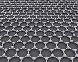
Fig. 1. Graphene is an atomic-scale honeycomb lattice made of carbon atoms (en.wikipedia.org).
3. Graphene Optical Properties
Graphene’s ability to absorb a rather large 2.3% of white light is also a unique and interesting property, especially considering that it is only 1 atom thick. This is due to its aforementioned electronic properties; the electrons acting like massless charge carriers with very high mobility. A few years ago, it was proved that the amount of white light absorbed is based on the Fine Structure Constant, rather than being dictated by material specifics. Adding another layer of graphene increases the amount of white light absorbed by approximately the same value (2.3%). [1] Due to these impressive characteristics, it has been observed that once optical intensity reaches a certain threshold (known as the saturation fluence) saturable absorption takes place (very high intensity light causes a reduction in absorption). This is an important characteristic with regards to the mode-locking of fibre lasers. Due to graphene’s properties of wavelength-insensitive ultrafast saturable absorption, full-band mode locking has been achieved using an erbium-doped dissipative soliton fibre laser capable of obtaining wavelength tuning as large as 30 nm. In terms of how far along we are to understanding the true properties of graphene, this is just the tip of the iceberg. Before graphene is heavily integrated into the areas in which we believe it will excel at, we need to spend a lot more time understanding just what makes it such an amazing material. Unfortunately, while we have a lot of imagination in coming up with new ideas for potential applications and uses for graphene, it takes time to fully appreciate how and what graphene really is in order to develop these ideas into reality. This is not necessarily a bad thing, however, as it gives us opportunities to stumble over other previously under-researched or overlooked super-materials, such as the family of 2D crystalline structures that graphene has born. [4]
4. Graphene Light Emitting Diode
Graphene has been hailed as a potential replacement for indium tin oxide (ITO) in the growing market for transparent conductors, in particular because it might enable the highly sought after flexible portable devices. Technological immaturity has so far hindered the widespread use of graphene as a transparent electrode, however researchers from Philips Research, the University of Cambridge, and Graphenea have engineered organic light emitting diodes (OLEDs) based on graphene which outperform state-of-the-art ITO devices. [1] The high electronic mobility and optical transparency of graphene make the material an excellent candidate for opto-electronic devices, such as solar cells, light emitting diodes (LEDs), and touch screens. Currently ITO is the most widely used material for such applications. However, the rising price and limited geographical availability of Indium, combined with the market trend in the direction of flexible devices, asks for alternative transparent conductors (TCs) for the next generation of devices. Although graphene offers a remarkably high mobility of charge carriers (for example electrons), the concentration of such carriers in graphene is generally low, leading to an overall unimpressive performance as an electrode. The process of doping the graphene layer with excess carriers is thus a necessary step in the production of graphene electrodes. Furthermore, in the case that the desired application is a transparent electrode, the doping process must preserve the high optical transparency of graphene. At least as important as the carrier concentration is the efficient exchange of charge carriers between the electrode and the active layer which actually performs the chosen opto-electronic function. The electronic bands of the electrode and active materials bend and adjust to each other, in turn reshaping the opto-electronic performance of the final device. It is thus important to study the band bending as well as the carrier exchange efficiency in actual complete opto-electronic devices. [5]
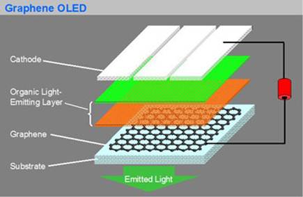
Fig. 2. Organic lighting-emitting diodes (OLEDs) with a few nanometer of graphene as transparent (www.nanowerk.com).
5. Graphene Nanotubes
Graphenated CNTs are a relatively new hybrid that combines graphitic foliates grown along the sidewalls of multiwalled or bamboo style CNTs. Yu et al .[6] reported on "chemically bonded graphene leaves" growing along the sidewalls of CNTs. Stoner et al. [7] described these structures as "graphenated CNTs" and reported in their use for enhanced supercapacitor performance. Hsu et al. further reported on similar structures formed on carbon fiber paper, also for use in supercapacitor applications. [8] Pham et al. [9] [10] also reported a similar structure, namely "graphene-carbon nanotube hybrids", grown directly onto carbon fiber paper to form an integrated, binder free, high surface area conductive catalyst support for Proton Exchange Membrane Fuel Cells electrode applications with enhanced performance and durability. The foliate density can vary as a function of deposition conditions (e.g. temperature and time) with their structure ranging from few layers of graphene (< 10) to thicker, more graphite-like. [11]
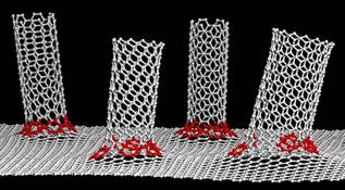
Fig. 3. A simulation of the graphene/carbon nanotube material, showing the covalent carbon bonds (www.extremetech.com).
The fundamental advantage of an integrated graphene-CNT structure is the high surface area three-dimensional framework of the CNTs coupled with the high edge density of graphene. Graphene edges provide significantly higher charge density and reactivity than the basal plane, but they are difficult to arrange in three dimensional, high volume-density geometry. CNTs are readily aligned in a high density geometry (i.e., a vertically aligned forest) [12] but lack high charge density surfaces—the sidewalls of the CNTs are similar to the basal plane of graphene and exhibit low charge density except where edge defects exist. Depositing a high density of graphene foliates along the length of aligned CNTs can significantly increase the total charge capacity per unit of nominal area as compared to other carbon nanostructures. [13]
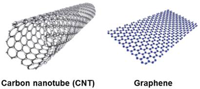
Fig. 4. Carbon nanotubes (CNT) and graphene are nano-sized carbon materials possessing various unique properties which can be applied for a range of applications. (polymer.kookmin.ac.kr).
6. Graphene Sensor
A sensor is a device that detects events that occur in the physical environment (like light, heat, motion, moisture, pressure, and more), and responds with an output, usually an electrical, mechanical or optical signal. The household mercury thermometer is a simple example of a sensor it detects temperature and reacts with a measurable expansion of liquid. Sensors are everywhere they can be found in everyday applications like touch sensitive elevator buttons and lamp dimmer surfaces that respond to touch, but there are also many kinds of sensors that go unnoticed by most like sensors that are used in medicine, robotics, aerospace and more. Graphene and sensors are a natural combination, as graphene’s large surface to volume ratio, unique optical properties; excellent electrical conductivity, high carrier mobility and density, high thermal conductivity and many other attributes can be greatly beneficial for sensor functions. The large surface area of graphene is able to enhance the surface loading of desired biomolecules, and excellent conductivity and small band gap can be beneficial for conducting electrons between biomolecules and the electrode surface. Graphene is thought to become especially widespread in biosensors and diagnostics. The large surface area of graphene can enhance the surface loading of desired biomolecules, and excellent conductivity and small band gap can be beneficial for conducting electrons between biomolecules and the electrode surface. Biosensors can be used, among other things, for the detection of a range of analytes like glucose, glutamate, cholesterol, hemoglobin and more. Graphene also has significant potential for enabling the development of electrochemical biosensors, based on direct electron transfer between the enzyme and the electrode surface. Graphene will enable sensors that are smaller and lighter - providing endless design possibilities. They will also be more sensitive and able to detect smaller changes in matter, work more quickly and eventually even be less expensive than traditional sensors. Some graphene-based sensor designs contain a Field Effect Transistor (FET) with a graphene channel. Upon detection of the targeted analyte’s binding, the current through the transistor changes, which sends a signal that can be analyzed to determine several variables? Graphene-based nanoelectronic devices have also been researched for use in DNA sensors (for detecting nucleobases and nucleotides), Gas sensors (for detection of different gases), PH sensors, environmental contamination sensors, strain and pressure sensors, and more.[14] [15]
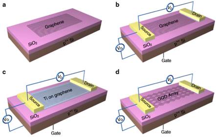
Fig. 5. Graphene photosensor (www.extremetech.com).
According to recent Graphene news, it will not be until 2030 when the biological applications of graphene will be fully-understood, basically because of the need to undergo numerous clinical trials and safety tests, among other requirements. The biocompatibility of the material also makes it an outstanding resource for tissue regeneration. More than its living tissue applications, It is also regarded as a viable option for creating bioelectric sensory devices, Which can be used in monitoring the levels of glucose and cholesterol in the body. Graphene applications can also be evident in anticancer treatments once it has been developed further. [16]
7. Graphene Energy Storage
One area of research that is being very highly studied is energy storage. While all areas of electronics have been advancing over a very fast rate over the last few decades, the problem has always been storing the energy in batteries and capacitors when it is not being used. These energy storage solutions have been developing at a much slower rate. The problem is this: a battery can potentially hold a lot of energy, but it can take a long time to charge, a capacitor, on the other hand, can be charged very quickly, but can’t hold that much energy. The solution is to develop energy storage components such as either a super capacitor or a battery that is able to provide both of these positive characteristics without compromise. Currently, scientists are working on enhancing the capabilities of lithium ion batteries to offer much higher storage capacities with much better longevity and charge rate. Also, graphene is being studied and developed to be used in the manufacture of super capacitors which are able to be charged very quickly, yet also be able to store a large amount of electricity. Graphene based micro super capacitors will likely be developed for use in low energy applications such as smart phones and portable computing devices and could potentially be commercially available within the next 5-10 years. Graphene-enhanced lithium ion batteries could be used in much higher energy usage applications such as electrically powered vehicles, or they can be used as lithium ion batteries are now, in smartphones, laptops and tablet PCs but at significantly lower levels of size and weight.[1] [17]
Fig. 6. Batteries graphene Li S energy storage (cleantechnica.com).
8. Graphene filter
Water is an invaluable resource and the intelligent use and maintenance of water supplies is one of the most important and crucial challenges that stand before mankind. New technologies are constantly being sought to lower the cost and footprint of processes that make use of water resources, as potable water (as well as water for agriculture and industry) are always in desperate demand. Much research is focused on graphene for different water treatment uses, and nanotechnology also has great potential for elimination of bacteria and other contaminants. Among graphene’s host of remarkable traits, its hydrophobia is probably one of the traits most useful for water treatment. Graphene naturally repels water, but when narrow pores are made in it, rapid water permeation is allowed. This sparked ideas regarding the use of graphene for water filtration and desalination, especially once the technology for making these micro-pores has been achieved. Graphene sheets (perforated with miniature holes) are studied as a method of water filtration, because they are able to let water molecules pass but block the passage of contaminants and substances. Graphene’s small weight and size can contribute to making a lightweight, energy-efficient and environmentally friendly generation of water filters and desalinators. It has been discovered that thin membranes made from graphene oxide are impermeable to all gases and vapors, besides water, and further research revealed that an accurate mesh can be made to allow ultrafast separation of atomic species that are very similar in size - enabling super-efficient filtering. This opens the door to the possibility of using seawater as a drinking water resource, in a fast and relatively simple way. [14] [18]
Fig. 7. Water Purification With Graphene Sheets (news.mit.edu).
9. Graphene Solar Panels
Graphene is made of a single layer of carbon atoms that are bonded together in a repeating pattern of hexagons. It is a 2 dimensional material with amazing characteristics, which grant it the title "wonder material". It is extremely strong and almost entirely transparent and also astonishingly conductive and flexible. Graphene is made of carbon, which is abundant, and can be a relatively inexpensive material. Graphene has a seemingly endless potential for improving existing products as well as inspiring new ones. Solar cells require materials that are conductive and allow light to get through, thus benefiting from graphene's super conductivity and transparency. Graphene is indeed a great conductor, but it is not very good at collecting the electrical current produced inside the solar cell. Hence, researchers are looking for appropriate ways to modify graphene for this purpose. Graphene Oxide (GO), for example, is less conductive but more transparent and a better charge collector which can be useful for solar panels. [19]
Graphene applications in solar cells and other sources of alternative energy have also generated a lot of buzz recently. In several studies completed in the past, Graphene has been classified as an excellent alternative to platinum, which is traditionally used in solar cells. Platinum is a very expensive material, which is why Graphene is a welcomed alternative because of its cost benefits. While it is cheaper, It is able to deliver the benefit of conductivity, Among others. Graphene applications in the field of alternative energy are expected to be more popular in the future as the demand for cleaner sources of energy becomes higher. [20]
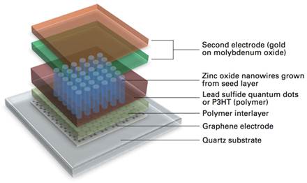
Fig. 8. Solar cell with nanowires and graphene electrode (mitei.mit.edu).
10. Graphene Aerogel
Graphene aerogel synthesis or production was achieved by expounding on the techniques that were previously used for making 2D Graphene films. This is actually the key behind the fact that Graphene aerogel is lighter than air. The Graphene component is usually comprised of one carbon atoms layer and researchers discovered that Graphene aerogel synthesis could be achieved through using an innovative freeze drying procedure to stack the atoms into 3D. Buy Graphene Aerogel And View Prices During drying Carbon nanotubes solutions are used And this removes the need to have a template, Which is the case with other aerogels. Among the main aerogel properties is that its size is determined be the container size in which it was built in. In addition, the nanotubes offer a stabilising benefit for smoother synthesis process. Graphene aerogel provides some of the most amazing benefits that may see it being used soon in most industries. For instance, among the major Graphene aerogel properties is that it is quite elastic and can easily retain its original form after some compression. In addition, Due to the lower density of Graphene aerogel, it is very absorbent, And it can even absorb more than 850 times its own weight. This means when future environmental clean-ups will be required, It will only comprise of spreading Graphene aerogel around the affected area and then it is picked up later after absorbing the organic products like oil. Beyond these environmental benefits of graphene aerogel this material may also have some applications in both the storage as well as the transfer of energy. Graphene is actually being studied for high thermal conductivity, and a lot more is expected from this product in the future. [21]
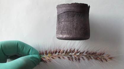
Fig. 9. Graphene aerogel, balancing on the spines of a plant (www.extremetech.com).
11. Graphene Knife
This will be more effective than the ordinary knife. A graphene knife will be very light and, therefore, easy to handle. This kind of a weapon will be easily carried in a pocket, ear lobe and even can be held between the fingers without feeling any weight. For those who love using swords, graphene sword will change the fighting experience for good. Graphene sword will be very light and easy to handle when compared to other ordinary swords. Graphene knife and Graphene sword will almost be invisible, and this means that they will not be easily noticed by the enemy. When it comes to effectiveness, graphene weapons will be the most effective on earth For instance; graphene sword is not easily broken and does not become blunt. This means that a graphene sword could be used to cut an ordinary sword as it cannot be easily damaged by heat or electricity current. Generally, graphene weapons will be several times effective when compared to the current version of weapons. Firstly, graphene is a very expensive material and buying a simple graphene knife could be as expensive as buying an automatic gun. On the other hand, production of graphene requires high technology that is not available in many parts of the world as at now. In order to manufacture affordable graphene swords, scientists need to come up with a less expensive way of producing graphene. However as at now, production of graphene for industrial use is at the first stage and scientists are not sure whether an economical way of producing graphene weapons will be discovered any time soon. Absurd to manufacture a graphene knife or a graphene sword after spending a lot of money in the production of graphene. Nevertheless, graphene could be used for production of high-tech graphene weapons such as war ships and aircrafts. Recent scientific reports have shown that superpower countries worldwide have shown interest to produce graphene weapons as was of maintaining their military supremacy. Generally, it is clear from the progress made by scientists from different parts of the world that graphene weapons have a bright future but the first stage is to discover how to produce graphene for commercial use. [21][22]

Fig. 10. Graphene weapons (http://www.aerogelgraphene.com).
12. Graphene Microphone
Scientists have developed a graphene based microphone nearly 32 times more sensitive than microphones of standard nickel-based construction. The researchers, based at the University of Belgrade, Serbia, created a vibrating membrane - the part of a condenser microphone which converts the sound to a current - from graphene, and were able to show up to 15 dB higher sensitivity compared to a commercial microphone, at frequencies up to 11 kHz. The results are published today, 27th November 2015, in the journal 2D Materials."We wanted to show that graphene, although a relatively new material has potential for real world applications" explains Marko Spasenovic, an author of the paper. "Given its light weight, high mechanical strength and flexibility, graphene just begs to be used as an acoustic membrane material." The graphene membrane, approximately 60 layers thick, was grown on a nickel foil using chemical vapour deposition, to ensure consistent quality across all the samples. During membrane production, the nickel foil was etched away and the graphene membrane placed in the same housing as a commercial microphone for comparison. This showed a 15 dB higher sensitivity than the commercial microphone. The researchers also simulated a 300-layer thick graphene membrane, which shows potential for performance far into the ultrasonic part of the spectrum. "The microphone performed as well as we hoped it would" adds Spasenovic. "A thicker graphene membrane theoretically could be stretched further, enabling ultrasonic performance, but sadly we're just not quite there yet experimentally."At this stage there are several obstacles to making cheap graphene, so our microphone should be considered more a proof of concept" concludes Spasenovic. The industry is working hard to improve graphene production - eventually this should mean we have better microphones at lower cost. [23]
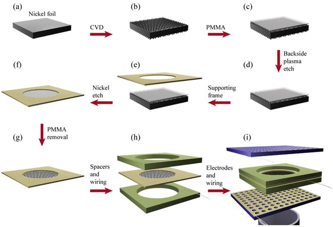
Fig. 11. Construction of graphene microphone.(engineering.unl.edu).
13. Graphene Radioactive Waste
Research collaboration between Russian and US chemists has discovered a new use for graphene oxide flakes—the clean-up of radionuclide contaminated water [24] [25]. Radioactive elements are harmful even in small concentrations, making any remediation of radioactive materials in water a slow process simply for the facts that very few radioactive particles may come in contact with reactants that have relatively little surface area for reaction. Graphene Oxide flakes inherently have large surface areas and are readily soluble in liquids. In addition to their large relative surface area, these nanothin particles have very fast sorption kinetics. These nanoflakes react with radioactive material including rare earth elements, plutonium, and uranium in liquids, attracting them to their surface and creating a precipitate in the liquid that is easily filtered [26]. The graphene oxide flakes are easily manufactured and display better sorption kinetics than bentonite clays or activated carbon filters used in conventional radioactive contaminated water cleanup. While the graphene does not eliminate the radioactive wastes, it concentrates the waste into a solid making it much easier to deal with. Graphene oxide is combustible, burning rapidly. This property allows the concentrated radioactive materials to be concentrated into dry solids that can then be repurposed and recycled for fuel or can be mined for their rare earth minerals in the case of water contaminated with radioactive actinides or lanthanides. Graphene Oxide is manufactured through a simple chemical reduction-oxidation (RedOx) method that requires mixing crystalline graphite with sodium nitrate, sulfuric acid, and potassium permanganate [27]. The formation of the thin films to create flakes is done by either chemical reduction with hydrazine, or bacterial synthesis; the latter being a "green" method free of additional chemicals. There are many potential benefits for the radionuclide sorption properties of graphene oxide flakes. Graphene oxide flakes could be used in the cleanup of radioactive water from nuclear accidents or during the decommissioning stage of nuclear energy production. Graphene oxide could be used in water treatment to reduce radioactive ionized mineral content in water from anthropogenic or natural sources. Graphene oxide flakes also offer promise for significant waste and cost reduction in oil and gas hydrofracturing; a process that often results in radioactive water contamination once the fracking fluids are extracted from the well. Additionally, graphene Oxide offers potential benefits in recovery of rare earth minerals from low concentration solutions. These benefits may help make nuclear energy safer, cost effectively reduce the risks of low carbon energy sources like natural gas, and reduce the resource and energy impacts in mining operations.
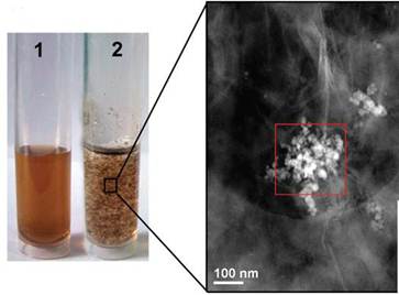
Fig. 12. Graphene Oxide for Nuclear Decontamination (www.i-sis.org.uk).
14. Graphene Quantum Dots Applications
Graphene quantum dots (GQDs) represent single-layer to tens of layers of graphene of a size less than 30 nm. Due to its exceptional properties such as low toxicity, stable photoluminescence, chemical stability and pronounced quantum confinement effect, GQDs are considered as a novel material for biological, opto-electronics, energy and environmental applications. The graphene quantum dot (GQD) is becoming an advanced multifunctional material for its unique optical, electronic, [28] spin, [29] and photoelectric properties induced by the quantum confinement effect and edge effect. GQDs are fragments limited in size, or domains, of a single-layer two-dimensional graphene crystal. Spectral studies have found that in almost all cases, GQDs are not single-layer graphene domains, but multi-layer formations containing up to 10 layers of reduced graphene oxide (rGO) from 10 to 60 nm in size. Presently, several techniques have been developed to prepare GQDs; these techniques mainly include electron beam lithography, chemical synthesis, electrochemical preparation, graphene oxide (GO) reduction, C60 catalytic transformation, the microwave assisted hydrothermal method (MAH), [30] [31] the Soft-Template method, [32] the hydrothermal method, [33] [34] [35] and the ultrasonic exfoliation method. [36]GQDs have various important applications in bioimaging, drug delivery, [37] LEDs lighter converters, photodetectors, OPV solar cells, and fluorescent material, biosensors fabrication.
15. Result and Discussion
Graphene is the thinnest material known to mankind, but it is also incredibly strong -- about 200 times stronger than steel. And yet, graphene can be made from graphite, also known as ordinary pencil lead. Described as a "one-atom thick layer of the layered mineral graphite," graphene only has two dimensions, making it the thinnest but strongest material ever created. Graphene is an excellent conductor of heat and electricity like silicon, but unlike silicon, graphene is not brittle, highly flexible, and conducts electricity much more efficiently. Although graphene can be derived from pencil lead, the material is actually very expensive. Graphene is one of the most diverse materials known to mankind, given how many of its properties are only exploited when graphene is combined with other elements, including gases, metals, and sources of carbon. Researchers from companies big and small continue to investigate and patent graphene to learn its properties and applications. Graphene is currently being tested to be used as ink, transistors, airplane wings, computer chips, batteries, flexible touch screens, anti-rust coatings, tires, DNA-sequencing devices, headphones, saltwater filters, tennis rackets, antennas, solar cells, paint, windows, and even living tissue applications such as bionic limbs. Graphene presents potential for a vast number of electronic and medical applications, including cars, buildings and cancer research. graphene, if perfected, can be used to build a quantum computer that can theoretically calculate all possible solutions at once at an infinitely faster computer speed.
References
- www.graphenea.com
- Smith, Paul. "Who Gives a Sheet about Graphene." Nanotech. L. & Bus. 10 (2013): 114.
- Stankovich, Sasha, et al. "Graphene-based composite materials." nature 442.7100 (2006): 282-286.
- Mas-Balleste, Ruben, et al. "2D materials: to graphene and beyond." Nanoscale 3.1 (2011): 20-30.
- www.graphenestakeholders.org
- Yu, Kehan, et al. "Carbon nanotube with chemically bonded graphene leaves for electronic and optoelectronic applications." The Journal of Physical Chemistry Letters 2.13 (2011): 1556-1562.
- Stoner, Brian R., et al. "Graphenated carbon nanotubes for enhanced electrochemical double layer capacitor performance." Applied Physics Letters 99.18 (2011): 183104.
- Hsu, Hsin-Cheng, et al. "Stand-up structure of graphene-like carbon nanowalls on CNT directly grown on polyacrylonitrile-based carbon fiber paper as supercapacitor." Diamond and Related Materials 25 (2012): 176-179.
- Pham, Kien-Cuong, et al. "The direct growth of graphene-carbon nanotube hybrids as catalyst support for high-performance PEM fuel cells." ECS Electrochemistry Letters 3.6 (2014): F37-F40.
- Pham, Kien-Cuong, et al. "Graphene-Carbon Nanotube Hybrids as Robust Catalyst Supports in Proton Exchange Membrane Fuel Cells." Journal of The Electrochemical Society 163.3 (2016): F255-F263.
- Parker, Charles B., et al. "Three-dimensional arrays of graphenated carbon nanotubes." Journal of Materials Research 27.07 (2012): 1046-1053.
- Cui, Hong-tao, O. Zhou, and Brian R. Stoner. "Deposition of aligned bamboo-like carbon nanotubes via microwave plasma enhanced chemical vapor deposition." Journal of Applied Physics 88.10 (2000): 6072-6074.
- Stoner, Brian R., and Jeffrey T. Glass. "Carbon nanostructures: A morphological classification for charge density optimization." Diamond and Related Materials 23 (2012): 130-134.
- www.graphene-info.com
- Kuila, Tapas, et al. "Recent advances in graphene-based biosensors." Biosensors and Bioelectronics 26.12 (2011): 4637-4648.
- Novoselov, Konstantin S., et al. "A roadmap for graphene." Nature 490.7419 (2012): 192-200.
- Goodenough, John B., and Kyu-Sung Park. "The Li-ion rechargeable battery: a perspective." Journal of the American Chemical Society 135.4 (2013): 1167-1176.
- Hu, Liangbing, and Yi Cui. "Energy and environmental nanotechnology in conductive paper and textiles." Energy & Environmental Science 5.4 (2012): 6423-6435.
- https://en.wikipedia.org
- Brownson, Dale AC, Dimitrios K. Kampouris, and Craig E. Banks. "An overview of graphene in energy production and storage applications." Journal of Power Sources 196.11 (2011): 4873-4885.
- www.aerogelgraphene.com
- Ci, Lijie, et al. "Controlled nanocutting of graphene." Nano Research 1.2 (2008): 116-122.
- http://phys.org/news/2015-11-graphene-microphone-outperforms-traditional-nickel.html
- Lotya, Mustafa, et al. "Liquid phase production of graphene by exfoliation of graphite in surfactant/water solutions." Journal of the American Chemical Society 131.10 (2009): 3611-3620.
- Romanchuk, Anna Yu, et al. "Graphene oxide for effective radionuclide removal." Physical Chemistry Chemical Physics 15.7 (2013): 2321-2327.
- Salas, Everett C., et al. "Reduction of graphene oxide via bacterial respiration." AcS Nano 4.8 (2010): 4852-4856.
- Yuan, Lizhi, et al. "Facile synthesis of silver nanoparticles supported on three dimensional graphene oxide/carbon black composite and its application for oxygen reduction reaction." Electrochimica Acta 135 (2014): 168-174.
- Ritter, Kyle A., and Joseph W. Lyding. "The influence of edge structure on the electronic properties of graphene quantum dots and nanoribbons." Nature materials 8.3 (2009): 235-242.
- Güçlü, A. D., P. Potasz, and P. Hawrylak. "Electric-field controlled spin in bilayer triangular graphene quantum dots." Physical review. B, Condensed matter and materials physics 84.3 (2011): 035425-1.
- Tang, Libin, et al. "Deep ultraviolet photoluminescence of water-soluble self-passivated graphene quantum dots." ACS nano 6.6 (2012): 5102-5110.
- Tang, Libin, et al. "Deep ultraviolet to near-infrared emission and photoresponse in layered n-doped graphene quantum dots." ACS nano 8.6 (2014): 6312-6320.
- Tang, Libin, et al. "Size-Dependent Structural and Optical Characteristics of Glucose-Derived Graphene Quantum Dots." Particle & Particle Systems Characterization 30.6 (2013): 523-531.
- Li, Xueming, et al. "Multicolour light emission from chlorine-doped graphene quantum dots." Journal of Materials Chemistry C 1.44 (2013): 7308-7313.
- Li, Lingling, et al. "Focusing on luminescent graphene quantum dots: current status and future perspectives." Nanoscale 5.10 (2013): 4015-4039.
- Li, Xueming, et al. "Sulphur doping: a facile approach to tune the electronic structure and optical properties of graphene quantum dots." Nanoscale 6.10 (2014): 5323-5328.
- Zhao, Jianhong, et al. "Chlorine doped graphene quantum dots: Preparation, properties, and photovoltaic detectors." Applied Physics Letters 105.11 (2014): 111116.
- Thakur, Mukeshchand, et al. "Milk-derived multi-fluorescent graphene quantum dot-based cancer theranostic system." Materials Science and Engineering: C 67 (2016): 468-477.


