
Chemistry Journal, Vol. 1, No. 3, June 2015 Publish Date: Apr. 22, 2015 Pages: 90-94
Study of Silver Nanoparticles Electroless Growth and Their Impact on Silicon Properties
R. Benabderrahmane Zaghouani*, L. Manai, B. Dridi Rezgui, B. Bessais
Photovoltaic Laboratory, Research and Technology Centre of Energy, Borj Cedria Science and Technology Park, Hammam Lif, Tunisia
Abstract
This work reports on the parameters influencing the growth of silver nanoparticles (Ag-Nps) on silicon intended to be used in many applications like silicon-based solar cells. Ag-Nps were deposited onto silicon substrates using Electroless Metal Deposition (EMD) in HF/AgNO3 solutions. The effect of the solution concentration and deposition time on the structural and optical properties of Ag-Nps was investigated. The nanoparticles were characterized by optical UV-VIS-NIR spectroscopy, Scanning Electron Microscopy (SEM) and Atomic Force Microscopy (AFM). Optical measurements show that the total reflectivity decreases in the UV-VIS-NIR spectral regions for Ag-Nps samples. In the UV-VIS region, this behavior can be explained by the excitation of the surface plasmons of the Ag-Nps, while in the NIR region it was attributed to light scattering from the Ag-Nps at the silicon substrate surface. SEM analysis shows that the variation of HF and AgNO3 concentrations leads to the growth of Ag-Nps having different average size and surface coverage. A minority carrier lifetime decrease in Ag-Nps/silicon samples is observed due to silver induced defects.
Keywords
Silver Nanoparticles, Electroless Metal Deposition, Plasmonic Effect, Reflectivity, Minority Carrier Lifetime
Received: March 27, 2015
Accepted: April 13, 2015
Published online: April 20, 2015
@ 2015 The Authors. Published by American Institute of Science. This Open Access article is under the CC BY-NC license. http://creativecommons.org/licenses/by-nc/4.0/
1. Introduction
Metal nanoparticles are used in many applications and for different goals. Deposited on the surface of silicon-based solar cells, they can efficiently reduce their surface reflectivity and increase the light absorption. In the last decade, many works demonstrated the utility of noble metals, especially silver and gold, in wafer-based [1] and thin-film solar cells [2-4]. The performance improvement of such cells is attributed to an increase of the optical path through a scattering mechanism from the metallic nanoparticles and to the increase of the optical absorption within the semiconductor via the enhancement of the localized electric field: it’s the plasmonic effect. The enhancement brought by these nanostructures depends strongly on many parameters such as the metal used, the size, the shape [5] and the environment surrounding the nanoparticles [6]. Metal nanoparticles are also used as metal catalyst to elaborate silicon nanowires (SiNWs) by the Metal Assisted Chemical Etching (MACE) method [7]. The metal solution concentration and then metal nanoparticles size are influencing the morphological SiNWs properties (length and diameter) and thus their optical end electrical behavior [8]. That’s why it’s important to control the parameters influencing nanoparticles deposition which depends on the method used. Metal nanoparticles can be deposited on silicon surface by different methods: evaporation [9], chemical deposition [10]. In this work, we report on the growth of silver nanoparticles (Ag-Nps) on silicon substrate by means of the Electroless Metal Deposition (EMD) in HF/AgNO3 solutions. The effects on the structural features of the nanoparticles of various experimental parameters such as HF and AgNO3 concentrations, deposition time and annealing were studied. We also discuss the impact of Ag-Nps on silicon properties which can modify the device response in which they are integrated.
2. Experimental Procedure
Silver nanoparticles were prepared by Electroless Metal Deposition in HF/AgNO3 solutions. The process consists of metal-plating a surface from a solution using chemical reducing agents. The substrate used is boron-doped single crystalline silicon with a resistivity of ~1-3 ohm.cmand a thickness of 300 µm. Before deposition of Ag nanoparticles, silicon substrates were cleaned with acetone for 1 min followed by immersion in ethanol for 1 min and rinsed in deionized water in order to eliminate organic greases. Finally, the substrates are etched in 5% HF for 5 min to eliminate native oxide. The substrates were then immersed in a HF solution containing AgNO3 with different HF and AgNO3 concentrations at ambient temperature and atmospheric pressure. The samples were then annealed under N2 gas at 250 °C during 60 min. The dependence of the morphological features of the deposited nanoparticles on the experimental parameters was investigated using a JEOL JSM-5400 Scanning Electron Microscopy (SEM) and a Digital Instruments Nanoscope 3100 Atomic Force Microscope (AFM) operating in tapping mode. The effect of the presence of Ag-Nps on the optical properties of the substrate (surface reflectivity) was analyzed using a PerkinElmer Lambda 950 UV/VIS spectrometer. The minority carrier lifetime is measured by the "Sinton WCT-120 lifetime tester" in the quasi-steady-state mode.
3. Results and Discussions
Silver nanoparticles are deposited by Electroless Metal deposition. When immersing silicon into the HF/AgNO3 solution, Ag+ ions capture electrons from silicon surface leading to Ag atoms due to the electronegativity difference between silver and silicon (Eq.1). Silicon underneath silver atoms is oxidized and is slightly etched by the hydrofluoric acid promoting metal deposition as depicted by (Eq.2).
![]() (Eq. 1)
(Eq. 1)
![]() (Eq. 2)
(Eq. 2)
The reaction continues giving rise to nanoparticles covering silicon surface. When using high HF concentration, the mechanism leads to the formation of silicon nanowires [11]. In this work, we use low HF concentrations. Fig. 1 shows SEM images plan-view of an Ag-Nps/silicon sample formed in a (5% HF+ 2mmol/L AgNO3) solution during 60 s (sample A). One may observe that most of the silicon surface is covered with Ag-Nps having irregular shapes and sizes (Fig. 1(a)). Annealing at 250 °C (below the melt temperature of silver (960°C)) during 60 min under N2 gas leads to the formation of quasi-spherical Ag-Nps having almost regular size with reduced surface coverage (Fig. 1(b)). This behavior is due to the fact that at a sufficient temperature annealing, elongated silver nanoparticles gain kinetic energy and mobility and then aggregate to form regular Ag-Nps [12]. Fig. 2 shows AFM images of the previous sample for two deposition times (40 s and 20 s). We notice that the different features of silver nanoparticles change gradually with increasing deposition time especially the size and the surface coverage. From AFM images, we obtain a surface roughness about 15 nm for the deposition time of 20 s and about 29 nm for the deposition time of 40 s. In addition, a reduction in Ag-Nps density is observed as the Ag-NPs diameter increases.
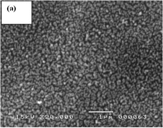
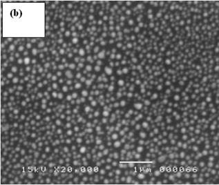
Fig. 1. (a) SEM images of sample A (5% HF+ 2mmol/L AgNO3) for a deposition time of 60 s(b)as-deposited and (b) annealed under N2 gas at 250 °C for 60 min
In order to study the solution concentration effect on nanoparticles deposition, we have varied HF and AgNO3 concentrations. Fig. 3 presents SEM images of sample A (5% HF+ 2mmol/L AgNO3), sample B (5% HF+ 6 mmol/L AgNO3) and sample C (0.5% HF+6 mmol/L AgNO3) for a deposition time of 60 s. One may notice that increasing AgNO3 concentration from sample A to sample B (fixed HF concentration) leads to a low nanoparticles surface coverage together with larger Ag nanoparticles. The average Ag-Nps size increases from about 125 nm for sample A to about 265 nm for sample B justified by a larger amount of Ag+ ions to be deposited on the surface of the sample B. However, it is worth noting that the decrease in HF concentration (from sample B to sample C) leads to lower Ag-Nps size for sample C with an average size of 200 nm due to the role of HF. These results highlight that the size, shape and Ag-Nps density can be controlled by simply adjusting the deposition parameters. Modifying both structural and morphological properties of the Ag-Nps influences surely the behavior of the silicon substrate.
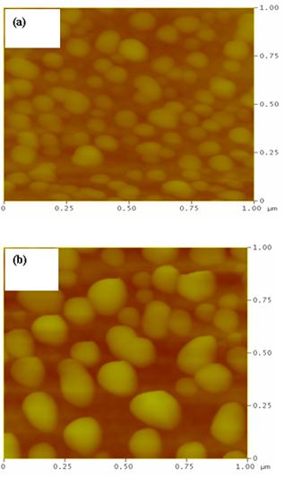
Fig. 2. AFM images (in tapping mode) of sample A (5% HF+ 2mmol/L AgNO3) showing the effect of the deposition time on the Ag-Nps: (a) td= 20 s and (b) td= 40 s.
Fig. 4 shows the surface reflectivity of sample A for three deposition times td (100 s, 60 s, 20 s). The presence of the Ag-Nps leads to a reflectance decrease as regard to the bare silicon substrate in the UV-VIS-NIR spectral regions. The reflectance decreases as the deposition time increases due to the increase of nanoparticles size. Two resonance peaks located in the UV-VIS spectral region are observed for td = 100 s and td = 60 s. These peaks indicate the excitation of localized surface plasmons in Ag nanoparticles caused by a collective oscillation of the conduction electrons under light [13] leading to an enhancement of electric field and then to the increase of light absorption [5]. The peak positioned nearly 300 nm corresponds to quadrupolar resonances, while peak at longer wavelength corresponds to dipolar resonances of Ag-Nps [9]. The peak of the dipolar-related band red-shifted from 480 nm to 500 nm as deposition time increases from 60 s to 100 s, respectively with a reflectance decrease about 5 %. The quadrupolar-related resonance peaks red-shifted from 305 nm to 310 nm showing a reflectance reduction of about 4 % while increasing the deposition time from 60 s to 100 s. For a deposition time of 20 s, the reflectivity spectrum shows broad bands with not well pronounced peaks, which is caused by the overlap of dipolar and quadrupolar resonance modes which could be caused by a large size distribution and a high surface coverage as been reported by Thouti et al. [9]. In the NIR spectral region, the reflectance decreases thanks to a further light trapping at the substrate surface via multiple scattering from silver nanoparticles causing an increase in the effective optical path length [5]. These results show that the absorption can be enhanced in the UV-VIS-NIR spectral regions when depositing silver nanoparticles on silicon surface. In previous works, similar effects on silver-MACE silicon nanowires were observed [11]. In Fig.5, we present the reflectance of sample A, sample B and sample C for a deposition time td of 60 s. For all samples, the reflectance decreases as regards to silicon substrate. Sample B, presenting a lower surface coverage as shown in Fig.3, has a higher reflectance than sample A and C. In the UV spectral region, sample A has a lower reflectance than sample C due to its higher surface coverage but in the visible sample C has almost the lowest reflectance. These results are explained by the fact that both surface coverage and nanoparticles size influence the reflectance response. We conclude that a controlled growth of silver nanoparticles can lead to a better reflectance decrease.
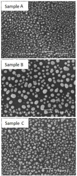
Fig. 3. SEM images of sample A (5% HF+ 2mmol/L AgNO3), sample B (5% HF+ 6 mmol/L AgNO3) and sample C (0.5% HF+6 mmol/L). The deposition time is fixed at 60 s
As shown above, a thin deposit of silver nanoparticles could reduce the reflections at silicon surface. A well-controlled growth of silver nanoparticles can offer an antireflection behavior which is interesting for photovoltaic applications. However, the presence of silver nanoparticles can generate defects at the surface of the active layer of the cell. These defects are potential recombination centers which are capable to trap generated carriers. Thus, the surface recombination could have an impact on the effective carrier lifetime and subsequently on the efficiency of the solar cells. The effective minority carrier lifetime τeff of the silicon substrates covered with Ag nanoparticles was measured using the WCT-120 photoconductance lifetime tester [14]. The τeff represents the impact of the different bulk recombination channels (Radiative, Auger and Shockley-Read-Hall recombination) and those related to the surface (recombination due to surface defects). The τeff can be expressed generally as (Eq.3):
![]() (Eq. 3)
(Eq. 3)
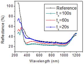
Fig. 4. Total reflectance of sample A for different deposition times. Reflectance of the bare silicon substrate is given for comparison
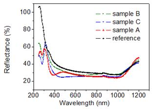
Fig. 5. Comparison of the reflectance of sample A , sample B and sample C for a deposition time of 60s.
In order to investigate the Ag-Nps effect on the effective minority carrier lifetime of the silicon substrates, the nanoparticles were deposited on both front and back surfaces for a deposition time of 60 s with the same conditions as the sample A. Fig. 6 presents the effective carrier lifetime as a function of the excess charge carrier density. For an excess carrier density of 2.1014 cm-3, τeff decreased from 1.26 µs for the untreated silicon substrate to 0.78 µs for Ag-Nps sample. This lifetime deterioration is due to the increase of surface recombination velocity caused by the presence of recombination centers generated by the Ag nanoparticles. The carrier lifetime is expected to decrease more when increasing silver nanoparticles density. This can be avoided by the use of a thin dielectric layer as a passivation layer between the silver nanoparticles and the substrate [2,15]. In this way, using silver nanoparticles can be beneficial in many applications such as silicon solar cells without deteriorating the electrical properties.
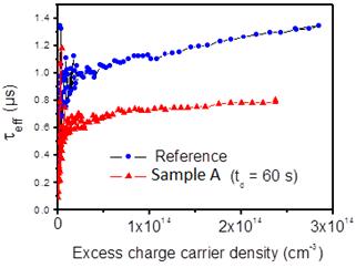
Fig. 6. Effective minority carrier lifetime of untreated silicon (reference) and sample A
4. Conclusions
In this work, we have explained the deposition mechanism of Ag nanoparticles on silicon substrates by immersion in HF/AgNO3 solution. It’s shown that the morphological features of Ag-Nps depend on experimental conditions (HF and AgNO3 concentrations, deposition time, annealing…). The optical properties of the silicon substrate may be tuned depending on the silver nanoparticles. It was found that Ag-Nps reduce the reflectance of silicon substrate and may enhance light absorption which can be beneficial for photovoltaic applications. However, it seems to be clear that further work is needed to avoid the degradation of the effective minority carrier lifetime of Ag-Nps covered silicon substrates.
References
- D.M. Schaadt, B. Feng, E.T. Yu, Appl. Phys. Lett. 86 (2005) 063106 (1-3).
- Y. Shi, X. Wang, W. Liu, T. Yang, R. Xu, Appl. Phys. Lett. 113 (2013) 176101 (1-3).
- Y.A. Akimov, W.S. Koh,Plasmonics. 6 (2011) 155-161.
- S. Pillai, K.R. Catchpole, T.Trupke, M.A. Green, J. Appl. Phys. 101 (2007) 093105 (1-8).
- H.A. Atwater, A. Polman, Nature Mater. 9 (2010) 205-213.
- K.R. Catchpole, A. Polman, Opt. Express. 16 (2008) 21793-21800.
- F. Bai, M. Li, D. Song, H. Yu, B. Jiang, Y. Li, Journal of Solid State Chemistry. 196 (2012) 596-600.
- M.Abouda Lachiheb,M.A. Zrir,N. Nafie,O. Abbes,J. Yakoubi,M. Bouaïcha, Sol Energy.110(2014)673-683.
- E. Thouti, N. Chander, V. Dutta, V.K. Komarala, J. Opt. 15 (2013) 035005(1-7).
- N.Bchtouli, S.Aouida, B.Bessais, Microporous and Mesoporous Materials. 187(2012) 82-85.
- R. Benabderrahmane Zaghouani, S. Aouida, N.Bchtouli, B.Bessais, Chemistry Journal.1 (2015) 10-14.
- K. Chan, Z. Aspanut, B. Goh, C. Sow, B. Varghese, S. Abdul Rahman, M.R. Muhamad, Appl. Surf. Sci. 257 (2011) 2208-2213.
- U. Kreibig, M. Vollme, Springer Series in Materials science, (1995).
- R.A. Sinton, A. Cuevas, M. Stuckings, Proc. 25th IEEE Photovoltaic Spec. Conf.(1996) 457-460.
- A. Centeno, J. Breeze, B. Ahmed, H. Reehal, N. Alford, Opt. Lett. 35 (2010) 76-78.


