
Physics Journal, Vol. 1, No. 2, September 2015 Publish Date: Sep. 2, 2015 Pages: 163-171
The Study of Microstructure and Creep Properties of Cu-Doped Sn-4wt%Ag and Sn-9wt%Zn Lead Free Solders with Annealing Temperature
A. Yassin1, E. Gomaa2, *
1Physics Department, Faculty of Education, Ain Shams University, Cairo, Egypt
2Physics Department, Faculty of Science, Ain Shams University, Abbassia, Cairo, Egypt
Abstract
The creep tests were conducted to investigate the effect of the heat treatments on the mechanical properties of Sn-4wt%Ag, Sn-4wt%Ag-0.5wt%Cu, Sn-9wt%Zn and Sn-9wt%Zn-0.5wt%Cu lead free solders. Samples were heat treated at temperatures of 373, 423 and 448 K to produce a range of different grain sizes. Constant-load creep tests were carried out at room temperature for each of the wire samples to all alloys. The results obtained show that there is a relationship between the heat-treatment temperature Ta and the microstructure and that this, in turn, affects the creep properties of the alloys. From the steady state creep rate the stress exponent is described in terms of the heat treatment temperatures. Comparisons are made with all alloys on the creep resistance of solder alternatives. The activation energy for all alloys are calculated at constant applied stress (σ = 9.75MPa). Furthermore, positron annihilation lifetime spectroscopy (PALS) has been applied to measure the variation of positron lifetime parameters for the above mentioned samples. The PAL results showed that value of 342 ps in Sn-9wt%Zn sample corresponding to a vacancy mean size of ~ 3 Ǻ. However, the values of positron annihilation lifetime of Sn-4wt%Ag alloy is shorter than its corresponding value of Sn-9wt%Zn alloy due to the dispersed Ag3Sn within the matrix which leads to a decrease in positron lifetime.
Keywords
Heat Treatments, Mechanical Properties, Microstructure, Activation Energy, Positron Annihilation
Received: August 1, 2015
Accepted: August 26, 2015
Published online: September 2, 2015
@ 2015 The Authors. Published by American Institute of Science. This Open Access article is under the CC BY-NC license. http://creativecommons.org/licenses/by-nc/4.0/
1. Introduction
A lot of efforts have been made to replace the conventionally used tin lead solders by new lead-free solder alloys due to the considerable toxicity of lead, health concerns, and environmental as well legislation reasons. Soldering technology has become indispensable for the interconnection and packaging of virtually all electronic devices and circuits. The SnAg, SnAgCu, SnZn and SnZnCu based alloys are some possible lead-free solders replacement for Sn–Pb. These alloys systems are quite important because they are generally recognized as the first choice for lead-free solders due to low cost and melting temperature [1]. Because of the industrial important applications of Sn-Zn and Sn-Ag alloys and the lack of information about the effect of grain diameter on its creep parameters, the mechanical properties of binary alloys Sn–Ag, Sn–Sb and Sn–Zn have been studied [2,3].
Heat treatment technique of alloys has a great effect on the resulting grain size [4]. The effect of grain size as well as ageing temperature on the steady state creep and microstructure parameters of Sn-1 wt% Zn alloy have been studied [5-8]. The steady state creep rate was found to decrease with increasing the grain size and was related to it by a Petch style relation.
SnAg alloys are being considered as one of the most favorable lead-free solder systems. In this respect numerous studies have been devoted to the microstructure of SnAg based alloys [9-13]. Gain et. al. [14], state that SnAgCu is one of the candidate solder alloys because of their relatively low melting temperatures and good thermal mechanical fatigue properties.
However, the results of a literature search revealed that the effect of isothermal heat treatment on the structure and mechanical properties of Sn-9wt%Zn alloy, showed that the crystallite size and lattice strain have opposite behavior with increasing annealing temperature due to recovery and recrystalization processes associated with the heat treatment process [15].
The present motivation is to explore further the experimental findings made by this group and to illuminate some light on the effect of annealing temperature on the steady state creep parameters of Sn-4wt% Ag, Sn-4wt% Ag-0.5wt%C u, Sn-9wt%Zn and Sn-9wt% Zn-0.5wt%Cu lead free solder alloys properties. Furthermore, positron annihilation lifetime spectroscopy (PALS) is used as a nondestructive tool to identify the type and fraction of nanoscale defects in these alloys. Also, the microstructure of the aged samples at (373K and 448K) for all alloys was studied micrographically.
PALS is a valuable nuclear method to study the microscopic structure of the materials [16,17]. PALS has a high sensitivity for probing vacancy defects of materials through measurements of positron lifetime of annihilation positron-electron pairs. It is based on high sensitivity of positron to localizing at low electron density regions of a material [18].
2. Experimental Work
Four different types of lead free solder alloys were examined. There compositions were Sn–4wt%Ag & Sn–4wt%Ag–0.5wt%Cu & Sn-9wt%Zn and Sn-9wt%Zn-0.5wt%Cu. They were prepared from high purity (99.99%) component materials. All components were melted under vacuum. Casting was done in a graphite mould and the ingot (rod of 12 mm diameter) was swaged to form wire samples of 0.8 mm diameter and 7cm in length. Each alloy samples were divided into three groups each group were annealed for 1hr at temperature of 373K, 423K and 448K respectively and then quenched in water at temperature of 298K.
Tensile creep tests were carried out with a computerize tensile testing machine. Creep tests were carried out at room temperatures (25oC) under different applied stresses ranging from 5.85 to 15.61MPa.
Scanning electron microscope (SEM) was used to characterize the microstructures of the various heat treatment conditions. Specimens were polished and etched in 2% initial for around 2 seconds.
The positron annihilation lifetime measurements have been performed in air at room temperature using fast-fast timing coincidence system with a time resolution full-width at half-maximum (FWHM) of 250 ps. A 11 μCi source of22NaCl deposited on a thin Kapton foil (7μm) was sandwiched between two identical specimens (1cm×1cm). For each spectrum, more than one million counts were accumulated. After source and background corrections, the lifetime spectra are fitted to a sum of exponential decay components convoluted with the Gaussian resolution function of the spectrometer:
![]()
where No is the total number of observed annihilation events and Ii denotes the relative intensity of the component having the lifetime τi. Only two components are resolved in our experimental spectra using the computer program LT 9.0 [19]. The shorter- lived component τ1 with intensity I1 represent the positron annihilating in the matrix and dislocations. The longer one τ2 with intensity I2 characterizes the annihilation of positrons trapped in vacancy clusters and three-dimentional monovacancies defects [20]
3. Results and Discussion
3.1. Creep Results
To evaluate the creep behavior of the four solder alloys Sn-4wt%Ag, Sn-4wt%Ag-0.5wt%Cu, Sn-9wt%Zn and Sn-9wt%Zn-0.5wt%Cu, creep property was testing at room temperature (25oC) with a range of applied stress (5.85 - 15.61MPa ). Fig. 1 (a, b and c) shows a typical set of creep curves for all lead free solder alloys wire specimens annealed at 373K, 432K and 448K respectively for 1h crept under constant applied stress of 9.75MPa. All tested solders show the expected creep characteristics. The creep curves each consist of a transient stage, which is characterized by a creep rate that decreases with time followed by a steady-state stage, where the creep rate is essentially constant. Specimens were not tested to failure. The figure shows that the creep rate decreases with increasing the annealing temperature. However, the results show that the Sn-4wt% Ag-0.5wt% Cu and Sn-9wt% Zn-0.5wt% Cu alloys had the highest creep resistance and lowest creep rate due to the presence of Ag3Sn, Cu6Sn5, Cu5Zn8 and CuZn5 IMCs in the eutectic areas in Sn-4wt%Ag-0.5wt%Cu and Sn-9wt%Zn-0.5wt%Cu alloys. Such behavior comes from the interaction between those IMCs with the dislocation motion [21]. It indicated that the Cu-addition is beneficial to improve the creep strength of the Sn-4wt%Ag and Sn-9wt%Zn solders and could enhance its creep resistance due to the Cu6Sn5 IMC.
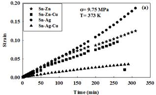
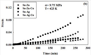
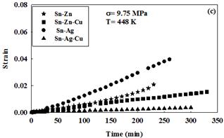
Figure 1. (a, b, c): Comparison creep curves at constant applied stress σ = 9.75MPa for Sn–4wt%Ag & Sn–4wt%Ag–0.5wt%Cu & Sn-9wt%Zn and Sn-9wt%Zn-0.5wt%Cu: (a) Ta=373K (b) Ta=423K (c ) Ta=448K.
The variations in creep rate, ![]() , suggest a basic change in the internal stress of the alloy sample during time. This implies that the hardening of the matrix was recovered immediately and balanced at an extended deformation rate [22].
, suggest a basic change in the internal stress of the alloy sample during time. This implies that the hardening of the matrix was recovered immediately and balanced at an extended deformation rate [22].
The steady-state creep rate,![]() , was determined from the slopes of the linear portions of the strain time curves of the type shown in Figure 1 (a, b and c) and using the relationship:
, was determined from the slopes of the linear portions of the strain time curves of the type shown in Figure 1 (a, b and c) and using the relationship:
![]() [1]
[1]
Where the stress exponent (n) can be evaluated from the slope of the ln![]() against ln σ as plotted in Figure 2 and according to the following equation,
against ln σ as plotted in Figure 2 and according to the following equation,
![]() [2]
[2]
The values of the stress exponent are given in table 1. Fig. 2 (a, b and c) shows the relationship between lnσ and ![]() (sec-1) for each alloy at different annealing temperature (373K, 423K, and 448K).
(sec-1) for each alloy at different annealing temperature (373K, 423K, and 448K).
Table 1. The stress exponent n for Sn-solder alloys at different annealing temperature.
| Stress exponent (n) | ||||
| Annealing Temp. (K) | SnAg | SnZn | SnZnCu | SnAgCu |
| 373 | 3.4 | 3.1 | 2.9 | 2.7 |
| 423 | 5.7 | 4.5 | 5.0 | 5.6 |
| 448 | 7.9 | 9.5 | 9.0 | 8.3 |
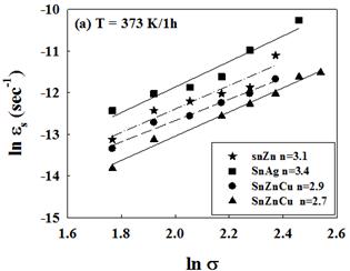
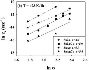
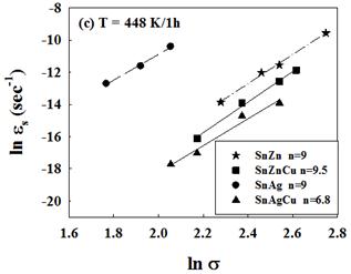
Figure 2. (a,b, c): The relationship between lnσ and ln![]() (sec-1) for all alloys at: ( a) Ta=373K, (b) Ta=423K and ( c) Ta=448K.
(sec-1) for all alloys at: ( a) Ta=373K, (b) Ta=423K and ( c) Ta=448K.
Table1 shows that, as the annealing temperature increases from 373K to 448K a significant increase in the stress exponent occurs which has been related to the dissolution of the β- phase during high temperature. The difference in the stress exponent values suggests that the creep deformation in the solder alloy is influenced by the formation of the IMCs that could restrict the dislocation climb at high annealing temperature. At low annealing temperature (373K) the stress exponent (n) is in the range (2.7-3.4) for all alloys. These values of the stress exponent (n) suggest that the creep deformation mechanism is due to viscous glide which in agreement with Linga Murty et al [23] and El-Bahay et al [24]. While at high annealing temperature (448K) the dislocation climb mechanism dominated because the n values for all alloys are in the range from (7.9-9.5).
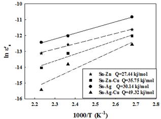
Figure 3. Relationship between 1000/T and ![]() of Sn–4wt%Ag & Sn–4wt%Ag–0.5wt%Cu & Sn-9wt%Zn and Sn-9wt%Zn-0.5wt%Cu solder alloys for determination the activation energy (Q) values.
of Sn–4wt%Ag & Sn–4wt%Ag–0.5wt%Cu & Sn-9wt%Zn and Sn-9wt%Zn-0.5wt%Cu solder alloys for determination the activation energy (Q) values.
Figure 3 shows the relationship between 1000/T (K-1) and ln ![]() (sec-1) at constant applied stress σ =9.75MPa for all alloys. The observed decrease in
(sec-1) at constant applied stress σ =9.75MPa for all alloys. The observed decrease in![]() with increasing the annealing temperature is due to the distribution of Zn-rich phase on the matrix which causes as obstacles to the mobile dislocations. The addition of Cu in the Sn-4wt%Ag and Sn-9wt%Zn alloys leads to form the irregular Cu6Sn5 IMC in the matrix which makes as dispersed particles which, act as obstacles to restrict the motion of grain boundaries and effectively hinder the dislocation movement within Sn bulk during the creep test.
with increasing the annealing temperature is due to the distribution of Zn-rich phase on the matrix which causes as obstacles to the mobile dislocations. The addition of Cu in the Sn-4wt%Ag and Sn-9wt%Zn alloys leads to form the irregular Cu6Sn5 IMC in the matrix which makes as dispersed particles which, act as obstacles to restrict the motion of grain boundaries and effectively hinder the dislocation movement within Sn bulk during the creep test.
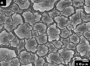
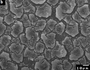
Figure 4 (a, b). SEM micrographs of Sn-4wt%Ag sample annealed at (a) 373K and (b) 423K for 1hr.
3.2. The Effect of the Heat Treatments on the Grain Size
The overall properties of the solder depend on the formed IMCs and the microstructure of the solder. It is therefore important to determine the types and morphology of formed IMCs.
The SEM micrographs of samples annealed at 373K and 423K for 1hr of Sn-4wt%Ag, Sn-4wt%Ag-0.5wt%Cu, Sn-9wt%Zn, and Sn-9wt%Zn-0.5wt%Cu alloys are shown in Figures 4, 5, 6 and 7. Generally, the micrographs of Sn-4wt%Ag-0.5wt%Cu, Sn-4wt%Zn and Sn-9wt%Zn-0.5wt%Cu alloys that annealed at two temperatures (373K, and 448K), show that the grain size decreases by increasing the annealing temperature. However, no change in the grain size with increasing the annealing temperature is observed for Sn-4wt%Ag (Figure 4). Clearly the effect of annealing temperature results in a reduction in the grain size of the Sn-4wt%Ag-0.5wt%Cu, Sn 9wt%-0.5wt%Zn and Sn-9wt%Zn-0.5wt%Cu due to the formation of the IMC particles of Cu6Sn5 in alloys. All of these microstructural changes have a potential effect on the creep properties.
Knowing that during the solidification of the eutectic Sn–4wt%Ag alloy the β-Sn dendrites and Ag3Sn eutectic coexist in the microstructure. The addition of 0.5wt%Cu into the eutectic Sn-4wt%Ag produce the large primary β-Sn grains surrounded by eutectic regions of two distinct IMC particles of Cu6Sn5 and Ag3Sn IMCs dispersed within the matrix as shown in Figure 5(a,b).
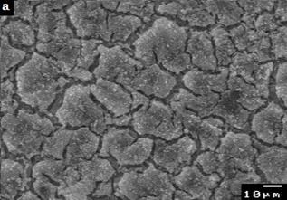
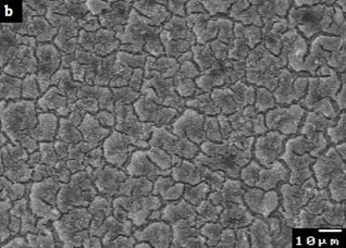
Figure 5 (a, b). SEM micrographs of Sn-4wt%Ag-0.5wt%Cu, sample annealed at (a) 373K and (b) 423K for 1hr.
Figure 6 (a,b) shows the microstructure of eutectic Sn-9wt%Zn which consists of β-Sn matrix (white gray regions) and α-Zn phase (dark gray phases) in the form of both fine particles and coarse needle-like Zn rich phase dispersed in the β - Sn matrix. With the addition of 0.5wt%Cu into the Sn–9wt%Zn solder alloy the rod-like dark grey phases of Cu6Sn5, Cu5Zn8 and CuZn5 IMCs are precipitated and also the α-Zn phase as shown in Figure 7 (a, b).
Figure 8 shows the effect of annealing temperature against the strain rate which indicated that by increasing the annealing temperature the strain rate decreasing, this is due to the decreasing in the grain size and increase the coarsening particles IMCs in the eutectic composition. In the Sn-9wt%Zn alloy the changes indicate that in the temperature range (373-448K) the β-Sn matrix phase dissolves which leads to increase the diffusion of Zn atoms to form the Zn-rich phase which causes a decrease in the strain rate![]() by increasing the annealing temperature. On the other hand, the strain rate
by increasing the annealing temperature. On the other hand, the strain rate![]() of Sn-4wt%Ag is greater than those other solders under investigation and is approximately 5.2 times that of Sn-4wt%Ag-0.5wt%Cu, 4.5 times than Sn-9wt%Zn and 2.3 times than Sn-9wt%Zn-0.5wt%Cu, this is because the Sn-4wt%Ag contains a Ag3Sn IMC in the matrix compared to the other solders whose have a fine particles like Zn-, and Sn6Cu5 phases. It is well known that, the presence of those fine particles in the eutectic phase shows much better creep resistance than Sn-4wt%Ag solder.
of Sn-4wt%Ag is greater than those other solders under investigation and is approximately 5.2 times that of Sn-4wt%Ag-0.5wt%Cu, 4.5 times than Sn-9wt%Zn and 2.3 times than Sn-9wt%Zn-0.5wt%Cu, this is because the Sn-4wt%Ag contains a Ag3Sn IMC in the matrix compared to the other solders whose have a fine particles like Zn-, and Sn6Cu5 phases. It is well known that, the presence of those fine particles in the eutectic phase shows much better creep resistance than Sn-4wt%Ag solder.
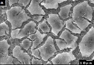
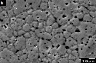
Figure 6 (a, b). SEM micrographs of Sn-9wt%Zn sample annealed at (a) 373K and (b) 423K for 1hr.
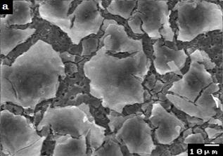
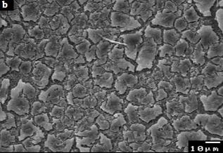
Figure 7 (a, b). SEM micrographs of Sn-9wt%Zn-0.5wt%Cu sample annealed at (a) 373K and (b) 423K for 1hr.
Figure 8. The relation between Ta(K) and ![]() for Sn-alloys.
for Sn-alloys.
Figure 9 shows the relation between the annealing temperature Ta (K) and the particle grain size, which shows that by increasing the annealing temperature the grain size decreases for all Sn-solder alloys as shown in table 2. Standard quantitative stereological techniques were used to determine the average dimensions (grain size) of β-tin phase [25].
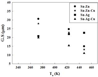
Figure 9. The relation between Ta(K) and G.S(µm) for Sn-alloys.
The effect of the annealing temperature in the Sn-4wt%Ag alloy, increases the number of the fine Ag3Sn IMC particles as a result of the dissolve of the β-Sn phase which decreases the strain rate.
Table 2. Grain diameter for all alloys at different annealing temperatures.
| Grain diameter (µm) | ||||
| Annealing Temp. (K) | SnAg | SnZn | SnZnCu | SnAgCu |
| 373 | 20.81 | 30.59 | 27.91 | 19.92 |
| 423 | 21.94 | 24.74 | 22.84 | 15.37 |
| 448 | 22.65 | 13.95 | 13.13 | 11.01 |
Table 3. The activation energy from the steady state creep for Sn- solder alloys.
| Solder | Activation energy (KJ/mol) |
| Sn-4wt%Ag | 30.14 |
| Sn-9wt%Zn | 27.44 |
| Sn-9wt%Zn-0.5Cu | 35.75 |
| Sn-4wt%Ag-0.5Cu | 49.52 |
3.3. Activation Energy
Since the deformation of polycrystalline materials at temperatures above 0.5Tm (where Tm is the melting temperature) takes place by different mechanisms, associated with different stress exponent (n) and activation energy (Q) values. Therefore, n and Q values are two important parameters for describing the deformation mechanisms of solders.
The activation energies of the steady state creep ![]() of Sn-4wt%Ag, Sn-4wt%Ag-0.5wt%Cu, Sn-9wt%Zn, and Sn-9wt%Zn-0.5wt%Cu lead free solder alloys are calculated from the slopes of the relation between 1000/T and ln
of Sn-4wt%Ag, Sn-4wt%Ag-0.5wt%Cu, Sn-9wt%Zn, and Sn-9wt%Zn-0.5wt%Cu lead free solder alloys are calculated from the slopes of the relation between 1000/T and ln![]() (Figure 3). All the results between 1000/T(K-1) and ln
(Figure 3). All the results between 1000/T(K-1) and ln![]() are in agreement with the equation of the steady state creep [26].
are in agreement with the equation of the steady state creep [26].
![]() = A exp (-Qs/KT). [3]
= A exp (-Qs/KT). [3]
The activation energies are summarizing in table 3.
The values of activation energy of the steady state creep has been estimated at constant applied stress (σ =9.75MPa) for Sn-4wt%Ag, Sn-4wt%Ag-0.5wt%Cu, Sn-9wt%Zn and Sn-9wt%Zn-0.5wt%Cu solder alloys. Table 3 shows, the apparent activation energy for Sn-4wt%Ag-0.5wt%Cu and Sn-9wt%Zn-0.5wt%Cu solder alloys are higher than those free Cu. This is attributed to the addition of Cu increased the barrier to the IMCs formation and have enhanced the formation of fine particles of new IMC Cu6Sn5 in the β -Sn matrix which makes an interaction with the dislocations during creep process. Accordingly, the activation energy of the present work are lower than that of lattice self diffusion which is about 100KJ/mol [27], but close to the dislocation pipe diffusion [28].
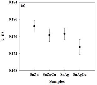
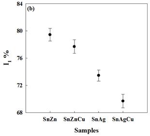
Figure 10. (a,b): Variation of (a) lifetime τ1and (b) relative intensity I1%, with the type of Sn alloys lead free samples.
3.4. Positron Annihilation
The positron annihilation lifetime components (t1, I1, t2 and I2) are shown in Figures 10 and 11. The values of lifetimes are related to defect size [18,20]. Figure 10 (a, b) shows that values of t1 are ranging from 173 ps to 178 ps and its relative intensities I1 are ranging from 69.7% to 79.4% in Sn alloys which is attributed to the presence of dislocations and small impurity vacancy clusters of two-dimensional character. The values of t1 are less than bulk lifetime of Sn which is 201ps [20]. The presence Sn–4wt%Ag & Sn–4wt%Ag–0.5wt%Cu & Sn-9wt%Zn and Sn-9wt%Zn-0.5wt%Cu. of Cu in the Zn alloys hinder dislocation formation which results in lower values of t1 and I1 of Sn-9wt%Zn-0.5wt%Cu and Sn-4wt%Ag-0.5wt%Cu alloys comparing to Cu free ones.
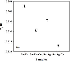
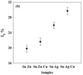
Figure 11. (a,b): Variation of (a) lifetime τ2 and (b) relative intensity I2 %, with the type of Sn alloys lead free samples.
Figure 11 (a, b), shows the positron lifetime in vacancy clusters, which described by the component t2. The values of t2 were found in the range from 326 ps to 342 ps indicating the presence of large vacancy clusters of five vacancies in these alloys [18,20]. Furthermore, the value of t2 is 342 ps in Sn-9wt%Zn sample corresponding to a vacancy mean size of ~ 3 Ǻ in this sample. On the other hand, I2 has a value of 19.8 % means that the defects concentration is low in this sample comparing to the other alloys. However, the effect of Cu particles on the positron lifetime can be seen in a considerably high in comparison to Sn alloys which free of Cu. The relatively small content of Cu atoms surrounding the excess vacancies leading to growth Cu6Sn5, Cu5Zn8, and CuZn5 which probably is responsible for the formation of nanoscale defects with a small size (t2) and high concentrations (I2). Therefore, the intensity (I2) which is a measure of the concentrations of defects is increased by an amount of 8.3% and 12% for Sn-9wt%Zn-0.5wt%Cu and Sn-4wt%Ag-0.5wt%Cu alloys respectively comparing to Sn alloys free of Cu. Generally, the values of positron annihilation lifetime (τ) of Sn-4wt%Ag alloy is shorter than τ of Sn-9wt% Zn alloy due to the dispersed Ag3Sn within the matrix which leads to a decrease in τ.
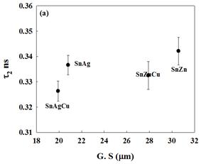
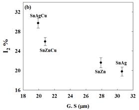
Figure 12. (a,b): Correlation of (a) lifetime τ2 and (b) relative intensity I2 %, with the grain size of Sn alloys lead free samples.
Correlation of second lifetime components (t2 and I2) which related to nanoscal size (τ2) of defects and its concentration (I2) with grain size (G.S) as well as stress exponent (n) are illustrated in Figure 12 (a, b) and Figure 13 (a, b) for all samples. It is clear that when the grain size increases the positron annihilated in defects have small sizes (τ2) and low concentrations (I2) at grain boundaries as shown in Figure 12 (a, b). As recommended by Dong et al. [29,30], when the grain size of the sample is increased the thickness of the grain boundaries is decreased. According to our results, there is opposite relation between the grain size and the size of defects as well as its concentrations (Figure 12 (a, b)).
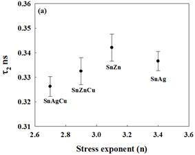
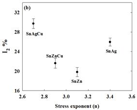
Figure 13. (a,b): Correlation of (a) lifetime τ2 and (b) relative intensity I2 %, with the stress exponential (n) of Sn alloys lead free samples.
On the other hand, one can observed that, there is a positive correlation between t2 and n while I2 correlated negatively with n as shown in Figure 13 (a, b). This indicated that, the size of defects (t2) increases with n whereas their number (I2) decreases. Furthermore, this correlation shows that Sn-4wt%Ag-0.5wt%Cu samples contains nonscale defects with small sizes and high numbers comparing to the other samples. This correlation confirms creep results where addition of Cu in the Sn-4wt%Ag and Sn-9wt%Zn alloys leads to form the irregular Cu6Sn5 IMC in the matrix which makes as dispersed particles which, act as obstacles to restrict the motion of grain boundaries and effectively hinder the dislocation movement within Sn bulk
4. Conclusions
In this paper, the effect of annealing temperature (373K, 423K, 448K) for 1h on the structure and mechanical properties as well as the positron annihilation lifetime parameters of Sn-4wt%Ag, Sn-4wt%Ag-0.5wt%Cu, Sn-9wt%Zn and Sn-9wt%Zn-0.5wt%Cu lead free solder alloys were investigated, the result showed that:
1. By increasing the annealing temperature the grain size decreases due to the dissolution of the β –phase and the increasing in the fine particles of IMCs.
2. The creep rate for all alloys was decreased continuously with increasing the annealing temperature.
3. Sn-4wt%Ag-0.5wt%Cu had the highest creep resistance due the fine dispersion of IMCs.
4. According to the obtained stress exponents and activation energies, creep is dominant by pipe diffusion –controlled climb for all investigated alloys.
5. Sn-9wt%Zn sample contains a vacancy with mean size of ~ 3 Ǻ.
6. Sn-4wt%Ag alloy contains defects with small size than its corresponding value of Sn-9wt%Zn alloy due to the dispersed Ag3Sn within the matrix.
Acknowledgements
The authors thank Dr. Emad Hassan Aly Department of Physics, Faculty of Science, Ain Shams University to assist them in the positron lifetime measurements.
References
- Y. Min, L. Xiuzhong, L. Xinghong, D. Jiahui, Conference Proceedings of 11th International Conference ICEPT-HDP (2010) 784-788.
- M. M.EL-Bahay, M. E. L.Mossalamy, M.Mahdy, A.A Bahgat, J. Mater. Sci .Mater. Electron. 15 (2004) 519–526.
- M. M. EL-Bahay, E.L.M. Mossalamy, M. Mahdy, A.A. Bahgat, Phys. Status SolidiA 198 (2003) 76–90.
- T. J. Chen, W. Wang, D. H. Zhang, Yongkum Ma, Yuzhou Hao, J. Alloys and Compounds, 546 (2012) 28 - 40.
- G. S. Al-Ganainy, M.T. Mostafa,Egypt. J. Sol. 23 (2000)2.
- H. R. Bakhsheshi-Rad, E. Hamzah, M. Medraj, M. H. Idris, A. F. Lotfabadi, M. Daroonparvar and M. A. M. Yajid, Materials and Corrosion (2014), DOI:10.1002/maco.201307492.
- S.B. Youssef, A. Fawzy, M. Sobhy, G. Saad, Acta Phys. Slov. 43 (1993) 431.
- B. Vilarinho, D. Soares, F. Castro, J. Alloys and Compound, 379 (2004) 161.
- C.M. Miller, I.E. Anderson and J.F. Smith, J. Electron. Mater. 23 (1994) 595.
- M.L. Huang and L. Wang, Metall. Mater. Trans. A 36 (2005) 1439.
- K. Mather, R. Patel, D. Raw, J. Wang, Y. Xing, L. Zavalij, P. Borgesen, E.J. Cotts, J. Electron. Mater. 33 (2004) 1429.
- S.K. Kang, W.K. Choi, D.Y. Shih, D.W. Henderson, T. Gosselin, A. Sarkhel, C. Goldsmith, K.J. Puttlitz, JOM 55 (2003) 61.
- K.S. Kim, S.H. Huh, K. Suganuma, Microelectron. Reliab. 43 (2003) 259.
- A.K. Gain, T. Fouzder, Y.C. Chan, A. Sharif, N.B. Wong. W.K.C. Yung, J. Alloys and Compd. 506 (2010) 216.
- M. Hammam, F. S. Allah, El Said Gouda, Y. El Gendy, H. Abdel Aziz, J. Eng. 2 (2010) 172-178.
- L.H. Su, C. Lua, L.Z. He, L.C. Zhang, P. Guagliardo, A.K. Tieu, S.N. Samarin, J.F. Williams , H.J. Li,Acta Materialia, 60 (2012) 4218.
- A.M. Samy, N. Mostafa, E. Gomaa,Appl. Surface Sci., 252 (2006) 3323.
- M.Misheva, N.Djourelov, FMA Margaca, IM. Miranda Salvado, J. Non-Cryst .Solids, 272 (2000) 209.
- J. Kancy, Methods Phys.Res, 374 (1996) 235.
- PP.Hautojarvi, C.Corbel, A. Dupasquier, A. P. Mills, Positron spectroscopy of solids, Jr (Eds), IOS Press, Amsterdam, 1995.
- A.A.El-Daly, A.E.Hammad, A. Fawzy and D.A.Nasrallh, Materials and Design 43 (2013) 40-49.
- A.A.El-Daly, A.Z.Mohamad, A. Fawzy, A.M.El-Taher, Mater. Sci. Eng. A 528 (2011) 1055-1062.
- K. Linga Murty, F.A.Mohamed, J.E. Dorn, Acta Met. 20 (1972) 1009.
- M.M.El-Bahay, M.E.El Mossalamy, M.Mahdy, A.A.Bahgat, J. Mater. Sci. 15 (2004) 519-526.
- E.E. Underwood. "Quantitative Stereology", Adison-Wesley, California, 1970.
- R.W.K. Honeycombe, The Plastic Deformation of Metals, Edward Arnold, (1984) 369.
- Geranmayeh A R,Nayyeri G. Mahmudi R, Mater Sci Eng A 547 (2012) 110.
- A. Hammad E, Mater.Desig. 52 (2013) 663-670.
- Y. Dong, L. Xiong, C. W. Lung, J Phys Condens. Matter. 3 (1991) 3155.
- A.M. Samy, E. Gomaa, N. Mostafa, The Open Ceramic Sci J 1 (2010) 1-4.


