
Physics Journal, Vol. 1, No. 2, September 2015 Publish Date: Aug. 5, 2015 Pages: 45-48
Defects Treatment in Silicon Diodes by Annealing with Pulsed CO2 Laser
Nafie A. Almuslet1, *, Saad A. A. Mohammed2
1Deapertment of laser systems, Institute of laser, Sudan University of Science and Technology, Khartoum, Republic of Sudan
2Electrical Engineering Department, Blue Nile University, Damazin, Sudan
Abstract
Defects arising from classical thermal annealing, electrical characteristics and dynamic resistance of silicon diode has been tried to treated by annealing with pulsed CO2 (λ= 10.6 µm) with pulse energy ranged from 500 to 600 mJ. Each diode was exposed to 5 pulses. The results showed an improvement in the behaviour of I-V characteristics curve of the diodes and reduction in its dynamic resistance.
Keywords
Laser Industrial Applications, Annealing by Laser, Silicon Diodes Annealing, CO2 Laser Applications
Received: July 7, 2015
Accepted: July 19, 2015
Published online: August 4, 2015
@ 2015 The Authors. Published by American Institute of Science. This Open Access article is under the CC BY-NC license. http://creativecommons.org/licenses/by-nc/4.0/
1. Introduction
High-energy ion-implantation is an increasingly favoured technique for retrograde profile buried-layer formation in advanced silicon processing. Crystal damage introduced by this doping technique can be removed by annealing. Short-time, high-temperature treatments, such as transient-rapid thermal annealing (T-RTA), is compatible with the requirement of low thermal budget processing. Analysis of doping and damage profiles of implanted silicon has been performed using a number of techniques, such as (cross-section) transmission electron microscopy ((X)TEM), secondary ion mass spectrometry (SIMS), Rutherford backscattering spectrometry (RBS), Secco etching C- T measurements or C- V measurements [1].
Laser annealing has been widely used for modification of semi-conductor surfaces. High power pulsed or continuous wave (CW) laser rapidly heats the surface regions to a high temperature or melts them above melting temperatures. After the termination of laser light, the surface regions rapidly cooled down. No substrate heating is necessary because laser irradiation energy effectively concentrates in the surface region during short irradiation time. Laser induced crystallization method has been developed and it has been applied for fabricating poly-crystalline silicon thin film transistor for flat panel display devices. Laser annealing also makes it possible to activate semiconductor implanted with doping atoms and diffuse doping atoms into semiconductor which is so-called laser doping. Laser induced activation is attractive to form shallow PN junction because of no marked impurity diffusion during short heating duration. Laser doping has been also paid attention for fabricating PN junction for solar cells .Laser annealing is also attractive for reduction of the density of interface traps at the semiconductor surface regions. Reduction of the density of interface traps by laser annealing at low processing temperature and in short tact time will be practical for semiconductor device processing. Especially for photo devices such as solar cells and high sensitivity photo sensors, a low annihilation rate of photo induced carriers is required. A simple surface passivation method will be important for photo device fabrication [2].
Pulsed laser annealing of semiconductors has been investigated extensively in recent years. The technique has the advantage that extremely high temperatures can be achieved at the surface without affecting the bulk of the semiconductor, even to the point where the semiconductor melts or material is removed by thermal evaporation. It is well known that the diffusivity of many ions is much greater in the molten state than in the solid, hence, pulsed laser annealing has been used to produce, e.g., highly doped surface regions by melting and thin film silicon-germanium alloys by melting and re-solidification of Ge on Si [3].
Laser annealing was considered to be the most advantageous for applying to film depositions on plastic substrates since laser irradiation with a short-time pulse can transmit energy to the target materials and avoid heating effects to the substrate. Therefore, the pulsed laser irradiation of an oxide film on a substrate appears to be the most suitable method for improving the crystallinity of the film with minimal thermal damage to the substrate [4].
2. Materials and Methods
Tables (1) and (2) show the type and specifications of the laser and materials used in this work. The materials used in this work are 6 samples of silicon diode.
Table 1. CO2 laser type and specifications.
| China | Country |
| Beijing Innobri Technology | Company |
| IB-601B | Model |
| CW + Pulsed | Laser Type |
| 10600 nm | Wavelength |
| 600mJ | Pulse Energy |
| up to 50 Hz | Pulse Repetition Rate |
| <10 ns | Width of Pulse |
| 30 W | Output power |
Table 2. Silicon diode parameters.
| Parameters | Symbol | Maximum Rating | Unit |
| Maximum repetitive peak reverse voltage | VRRM | 50 | V |
| Maximum RMS voltage | VRMS | 35 | V |
| Maximum DC blocking voltage | VDC | 50 | V |
The samples were irradiated by the CO2 laser with wavelength of 10.6 µm and energy of 500, 520, 540, 560, 580, and 600 mJ, respectively. Each diode was exposed to 5 pulses from the CO2 laser.
3. Results and Discussion
Figure (1) shows the I-V characteristics of the silicon diodes irradiated 5 times for each diode by pulsed CO2 laser with energy ranged from 500 to 600 mJ. The values of voltage drop across each diode corresponding to its current value are listed in table 3, and the relationship between the dynamic resistances, which were calculated from I-V characteristics curve for each diode, is plotted in figure (2).
From figure (1), one can see the deviation of the curve of the silicon diode before annealing from other curves due to the defects after furnace annealing. The diodes treated by energies of 500, 520, 540, 560, 580, and 600 mJ, respectively, exhibits forward voltage of 0.605, 0.6, 0.6, 0.595, 0.593, and 0.588 V at 10 mA.

Figure 1. I-V characteristics for diodes irradiated by single pulse from CO2 laser with different energies.
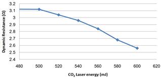
Figure 2. The dynamic resistance of the diodes irradiated with single pulse of CO2 laser with different energies.
The electrical conductivity of the silicon diodes changed as the laser energy increased from 500 to 600 mJ, because the carrier concentration is changed along with the increasing of laser energy. These results can be explained in terms of carrier trapping by the localized trap states at the grain boundary and the reduction of the trap state density with increasing laser energy. The trap state density also changed along with the number of laser pulses. By increasing the number of pulses, the trap state density can be reduced [5].
Dynamic resistance of the silicon diodes in figure (2) decreased gradually from 3.16 to 2.56 Ω. This reduction can be explained as follows:
The grain size increased and the amorphous portion decreased, so that, less trapping states will exist in poly-Si films with big crystalline grains. Trap densities are often given as a volume density thus averaging over various trapping depths. The spectral density of localized states in the band gap, i.e., the trap densities as a function of energy _trap density of states ,trap (DOS), gives a much deeper insight into the charge transport and device performance. This leads to a higher free carrier concentration, which reduces the resistivity and leading to decrease the dynamic resistance of the silicon diode. A large number of defects arising after furnace annealing due to incomplete atomic bonding exist in the grain boundaries, which forms trapping states. This reduces the number of free carriers available for electrical conduction. After trapping the mobile carriers, the traps become electrically charged and they create a potential barrier, which impedes the motion of carriers from one grain to another. The amorphous phase is also an insulating region, which implies in another potential barrier [6,7]. All these factors can affect negatively the behaviour of I-V characteristics of silicon diode.
Laser annealing of Si has been demonstrated to offer advantages over furnace annealing such as exceeding the solid solubility limit of dopants in Si and having less defects after annealing. Pulse lasering results in faster actuation response than conventional furnace annealing or continuous wave (CW) laser - treatment. Advantage of laser annealing is development of a biasing force which results in a back-to-preliminary- state tendency not achievable in traditional heat treatment processes. Laser heating results in formation of thermo elastic crystalline areas surrounded with wide amorphous regions exploitable in design of many functional systems. Furnace cooling can decrease the residual stresses that may remain throughout the layer [8].
Most of the studies have been carried out on nanosecond laser pulses. This ns laser pulses provide fluences (energy densities) high enough to melt a surface layer of amorphous Si created by ion implantation of dopants on single crystalline silicon [9]. For both single crystalline Si (c-Si) and polycrystalline Si (poly-Si), the effect of dopant concentration on resistivity is essentially the same. Greater concentrations of carriers equate to lower resistance [10].
4. Conclusions
The effect of laser annealing method to investigate the silicon diode was used and discussed. The obtained results showed that the defects arising after conventional annealing were decreased gradually after laser annealing, and the electrical properties such as I-V characteristics and dynamic resistance were improved after laser irradiation when they treated with energies ranged between 500 to 600 mJ from pulsed CO2 laser. The results showed that the dynamic resistance reduced from 3.12Ω to 2.56Ω, and the voltage drop falls from 0.7 V before irradiation to 5.88 V after irradiation.
Annealing by pulsed CO2 laser introduced improvements in the electrical properties of diode such as I-V characteristics and dynamic resistance.
In conclusion, the infrared lasers such CO2 laser annealing is an important technique in the semiconductor industrial for improving the device performance. This result is potentially important to the improvement of semiconductor device's performance for both semiconductor industry and other possible research avenues.
Acknowledgement
There are many people who we need to thank and acknowledge for their contribution towards this work. We are grateful to all the staff at the institute of laser in Sudan University of Science and Technology.
References
- J. G. E. Klappe , I. Bfirsony. Optimization of ion implantation damage annealing by means of high-resolution X-ray diffraction., Thin Solid Films, 235 (1993) 189-197
- T. Sameshimaa, M. Hasumia, and T. Mizuno. Laser annealing of plasma-damaged silicon surface. Applied Surface Science 336 (2015) 73–78
- D. Sands, J.E. Nicholls, J.H.C. Hogg S. Chalk, F.X. Wagner, W.E. Hagston, et al. Pulsed laser annealing of CdTe/CdMnTe super-lattices. Journal of Crystal Growth 184/185 (1998) 114-l 18
- Te-Wei Chiu, Kazuhiko Tonooka, Naoto Kikuchi.Fabrication of ZnO and CuCrO2:Mg thin films by pulsed laser deposition with in situ laser annealing and its application to oxide diodes.Thin Solid Films 516 (2008) 5941–594.
- Seiichiro Higashi, Kentaro Ozaki , and Keiji Sakamoto et al. "Electrical Properties of Excimer-Laser-Crystallized Lightly Doped Polycrystalline Silicon Films". Jpn. J. Appl. Phys. Vol.38 (1999) 857–860.
- TEIXEIRA, R.C.; DOI, I.; ZAKIA, M. B. P.; SWART, J. W.; DINIZ, J. A. Grain. Size Influence on Sheet Resistance of P- and AS-Implanted Polycrystalline Silicon Deposited by Vertical CVD Reactor, Centre for Semiconductors Components – State University of Campinas, R. Pandiá Calógeras, 90, CEP: 13083-970, Caixa Postal 6061, Campinas – SP – Brasil (2002).
- Wolfgang L. Kalb, Simon Haas, Cornelius Krellner, Thomas Mathis, and Bertram Batlogg. Trap density of states in small-molecule organic semiconductors: A quantitative comparison of thin-film transistors with single crystals. PHYSICAL REVIEW B 81, 155315 (2010).
- S K SADRNEZHAAD, NOUSHIN YASAVOL, MANSOUREH GANJALI, and SOHRAB SANJABI. Property change during nanosecond pulse laser annealing of amorphous NiTi thin film. Bull. Mater. Sci., Vol. 35, No. 3, June (2012), pp. 357–364.
- D. V. Tran; Y. C. Lam; H. Y. Zheng; V. M. Murukeshan; J. C. Chai; D. E. Hardt. Femtosecond laser processing of crystalline silicon", published on Optics and Lasers in Engineering (2004).
- Sidan Jin, "Boron Activation and Diffusion in Polycrystalline Silicon with Flash- Assist Rapid Thermal Annealing", A dissertation presented to the graduate school of the university of Florida in partial fulfilment of the required for the degree of Doctor of Philosophy, university of Florida (2011).


