
International Journal of Modern Physics and Applications, Vol. 1, No. 4, September 2015 Publish Date: Jul. 20, 2015 Pages: 131-138
Contact Resistance in Organic Thin Film Transistors: Application to Octithiophene (8T)
S. Zorai*, R. Bourguiga
Physics laboratory of Materials: Structure and Properties, Group of Physics Components and Nanometric Devices, Carthage University, Faculty of Sciences of Bizerte, Jarzouna-Bizerte, Tunisia
Abstract
In this paper, we present a device model of the charge distribution and the contact resistance in organic thin film transistor (OTFTs) in which the active layers are made of octithiophene. In this model we suppose that the current in organic semiconductors is only carried by injected carriers from the electrodes and an analytical formulation for the charge distribution inside the organic layer was derived.
Keywords
Thin Film, Organic Semiconductors, Contact Resistance, Active Layers
Received: June 5, 2015
Accepted: June 13, 2015
Published online: July 16, 2015
@ 2015 The Authors. Published by American Institute of Science. This Open Access article is under the CC BY-NC license. http://creativecommons.org/licenses/by-nc/4.0/
1. Introduction
Organic thin-film transistor (OTFT) was first fabricated in 1986 by Tsumura et al. [1] with electropolymerized polythiophene as the semiconducting active layer. Since then the performance of OTFTs has been enormously improving [2–7]. Compared with their inorganic counterparts, organic materials possess great advantages, such as inherent compatibility with plastic substrates, flexibility and amenability to low-cost and low temperature processed methods such as melt processing, printing and solution deposition, so that OTFTs have potential applications in radio frequency identification (RFID) tags [8,9], flexible displays [10,11], electronic papers [1, 12] and sensors [13].
The conductive polymers are very attractive materials for building electronic devices such as flat panel displays [14,15]. They were the subject of a particular attention of the industrial and scientific community because of the vast fields of investigation that they offer in the fundamental domain as well as in the applied one. In the past few years, the performance of organic thin film transistors (OTFTs) has been considerably improving [16–18]. Among the conjugated oligomers used as active materials in the fabrication of OTFTs, octithiophene is one of the most promising materials due to its high field-effect mobility [18,19]. The performance of octithiophene-based OTFTs is observed to be compared to that obtained from hydrogenated amorphous silicon TFTs [19,20].
Since the contact between the electrode and the organic is one of the most important factors in determining the device performance, it is imperative to investigate and to understand the symmetry of interface formation in the cases of metal deposited onto organic and organic deposited onto metal.
In this paper, we present a physical device model for organic thin film transistors based on polythiophene. We develop analytical equations for the two-dimensional charge distribution by solving Poisson’s and transport equations and by applying boundary conditions for a finite thickness semiconductor. The carrier-density in the transition zone at the source-organic semiconductor interface is modeled to build up a formulation of Rc as an integration of the local resistivity. Numerically calculated Rc clearly shows the influence of Vg and injection barrier height (Eb) on the determination of Rc.
2. Operation Mode: Layer Structure of Polymers in the Conduction Channel
Organic thin-film transistors based on polythiophene were built on thermally oxidized highly doped wafers [17]. The highly doped substrate acts as the gate electrode. The silicon oxide layer had a capacitance of 8 nF cm−2. An organic semiconductor layer was deposited on the silicon oxide by vacuum evaporation at a base pressure of 5 × 10⁻⁴ Pa. The deposition rate was around 5 nm per min, and the substrate was kept at a temperature of 150 ◦C during deposition. This procedure is used to give highly oriented polycrystalline films with all molecules pointing close to the normal of the substrate.
The devices were completed by evaporation gold source and drain contacts through a shadow mask. The channel length Z = 5000 μm and the width L = 50 μm.
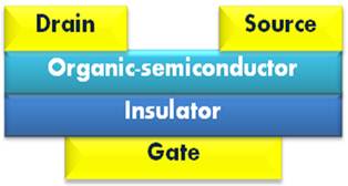
Fig. 1. Schematic view of organic thin film transistor.
A typical organic thin-film transistor (OTFT) is composed of three electrodes: drain, source and gate, a dielectric layer, and an organic semiconductor layer (Fig. 1).
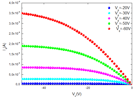
Fig. 2. Output characteristic of octithiophene thin film transistor drain current via drain voltage for different gate voltage.
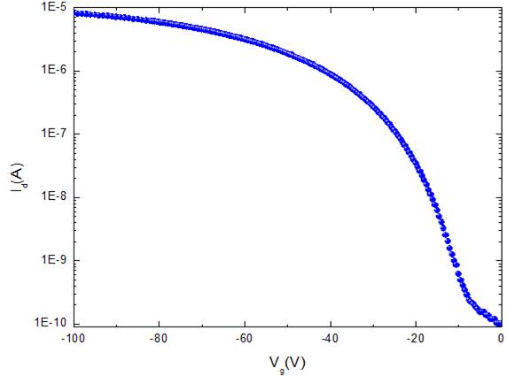
Fig. 3. Transfer characteristic drain current via gate voltage at 300K.
Fig. 2 and fig.3 shows the output (variation of drain current via drain voltage at different gate voltage) and transfer characteristic (variation of drain current via gate voltage at constant drain voltage) for OTFTs based on polythiophene at room temperature.
This architecture looks similar to the conventional silicon metal-oxide-semiconductor field effect transistors (MOSFETs) what basically differ from the classical inorganic semiconductor OTFTS are the electronic properties [21-23]. Two different voltage sources are used: Vg is the gate voltage and Vd is the drain voltage. In order to derive an analytical expression of the OTFTS’s steady-state current, it is assumed that the current transport is parallel to the semiconductor-insulator surface.
3. Theoretical Model of Charge Distribution in Organic Semiconductor
In order to know how the injected holes from the source (ρs) and the gate-induced holes at the channel (ρc) are distributed along the thickness of the organic layer, we develop a two dimensional model based on three suppositions:
• Hole-only conduction is considered.
• Gradual channel approximation holds.
• All charge carriers are "injected" into the organic semiconductor.
3.1. Preliminary Theory
In this part we consider an unintentionally doped organic semiconductor is fully depleted so that the above assumption for all charge carriers are injected into the organic semiconductor can be made [24]. So, an organic semiconductor is rather an insulator that can only ‘transport’ the carriers given by external circumstances and the classical theory on the metal/insulator junction that has been intensively dealt with in the early days of solid-state electronics through the 1940s and 1950s can be modified.
The electrostatic distribution of injected carriers ρ(x) can be estimated by simultaneously analyzing Poisson’s (given by equation (1)) and the transport (drift-diffusion) (given by equation (2) because we suppose a one-dimensional insulator in contact with a metal electrode (which is charge reservoir) at x = 0 that extends toward the positive x-direction up to x = ts where ts is the thickness of the semiconductor.
![]() (1)
(1)
![]() (2)
(2)
Where ρ(x) is the hole concentration, F the electric field, ε the permittivity of the organic semiconductor, q the elementary charge, µ the hole mobility, J the hole current density. The hole diffusion coefficient D is given by the Einstein relation ![]() where KB is the Boltzmann constant and Ta is the absolute temperature.
where KB is the Boltzmann constant and Ta is the absolute temperature.
The expression of current density is obtained by substituting equation (1) in equation (2) and using the Einstein relation may be expressed as:
![]() (3)
(3)
This is the fundamental equation of the given physical system to be solved. At thermal equilibrium, the net current is zero (the drift current and the diffusion current compensate each other) so that
![]() (4)
(4)
So equation (4) can be integrated once to
![]() (5)
(5)
Where ψ is an integration constant.
The first solution of equation (5) is derived by Mott and Gurney for a semi-infinite semiconductor (ts→∞) [14]. So, when x →∞ both F(x) and dF=dx equal to zero. Consequently the solution for the electric field is reached by separating variables is given by equation (6) where ![]() is the electric field at the junction x=0 and x0 is an integration constant.
is the electric field at the junction x=0 and x0 is an integration constant.
![]() (6)
(6)
The first derivative of equation (6) gives us the whole distribution
![]() (7)
(7)
Where ![]() is the hole distribution at the junction x=0 and
is the hole distribution at the junction x=0 and![]() . The value of x0 can be calculated from the boundary value of either F0 or ρ0.
. The value of x0 can be calculated from the boundary value of either F0 or ρ0.
In equation (7), we see good if the initial carrier density ρ0 is high x0 became smaller. So if x0 is small, the carriers are densely concentrated at the junction and do not spread far away from the injecting surface. Despite the Mott-Gurney model provides meaningful insight into the charge distribution, its usage should be limited to very think organic crystals and this model cannot be safely applied to thin organic films.
The more general solution of equation (5) is developed for the first time by Skinner [25]. It means that one can challenge the ‘finite’ junction without forcing ψ to zero. In the following we separated the cases by the sign of the integration constant and obtained separate sets of solutions depending on this sign. An essential boundary condition for the finite semiconductor is F(ts) = 0 because there cannot be any current flowing into or out of the semiconductor at the surface y = ts. The injected holes (positive charges) make the only contribution to the space charge in Poisson’s equation. Consequently, the sign of dF=dx is always positive through the whole semiconductor thickness. In other words, F (0) is negative and F(x) approaches zero from x = 0 to x = d. At x = ts, F becomes zero by the boundary condition and dF = dx remains positive. Therefore, the right-hand term in (5) is negative and the corresponding solution is the trigonometric function in [25], which can be given by :
![]() (8)
(8)
![]() (9)
(9)
To calculate the value of the constant ψ, we introduce the boundary condition if x=ψ, F (ψ) = 0. So equation (8) gives:
![]() (10)
(10)
By using the trigonometric identities we obtain:
![]() (11)
(11)
by replacing the expression (11) in equation (9), the expression of the hole concentration may be expressed as for ts<x<0:
![]() (12)
(12)
3.2. Solutions for the Model
3.2.1. Charge Distribution
In spite of the model studied previously gives exact solutions for thin-film cases, the equation (11) does not lead to an analytical expression for ψ and the final solution requires numerical computation.
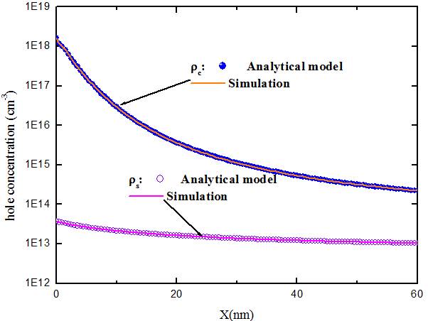
Fig. 4. Injected holes from the source (ρs) and the gate-induced holes at the channel (ρc) via the thickness of organic layer.
Now let us return to the two-dimensional semiconductor and discuss how the initial carrier densities at the insulator/semiconductor interface (x = 0) are determined in the OTFT architecture in fig. 4. The carrier density at a metal/semiconductor interface is dictated by Boltzmann’s statistics [26] so that the source carrier density at y = 0 ρs0 is strongly injection-limited following
![]() (13)
(13)
The hole barrier height Eb corresponds the energy between the electrode Fermi level and the semiconductor HOMO level and σƲ is the effective density of states at the HOMO edge. On the other hand, the channel carriers are induced by the gate capacitance and given by:
![]() (14)
(14)
Where Cox is the insulator capacitance per unit area, Vth the threshold voltage and Qtot the total channel charge per unit area.
The channel hole concentration at x = 0 is approximate to:
![]() (15)
(15)
From equation (7) we deduce the two expressions of the characteristic distribution lengths for the source and the channel charges
![]() (16)
(16)
![]() (17)
(17)
In fig.5 and fig. 6 we present respectively source distribution factors (ρs0 and xs0) as a function of Eb and channel distribution factors (ρc0 and xc0) as a function of gate voltage using equation (13) and (15) with σƲ = 1.811012 cm-3, T = 300 K, ε= 3ε0 and Cox = 8nFcm-2.. The solid lines indicate the initial hole concentrations and the dashed lines correspond to the distribution lengths. Fig. 5 and fig. 6 shows the reliability of the approximate solutions.
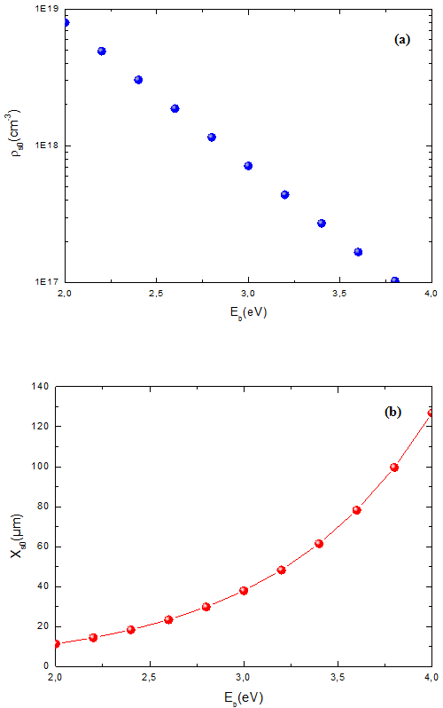
Fig. 5. Variation of Source distribution parameters ρs0 (a) Xs0 (b) via hole barrier height Eb
The variation of ρs0 is much lower than ρc0 due to the high injection barrier. Another key feature of fig. 5 and fig. 6 is that xs0 normally exceeds the thickness of an organic thin-film, whereas xc0 is far smaller than the film thickness. This finding enables an independent modelling of the source and channel distribution of charges by means of an approximation method.
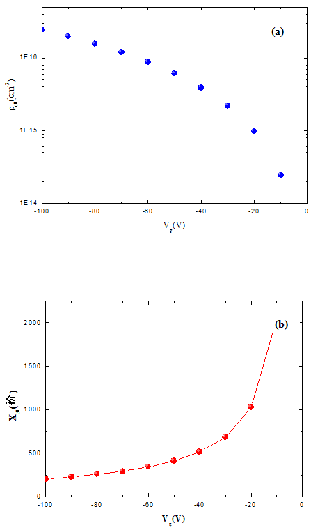
Fig. 6. Variation of channel distribution parameters ρc0 (a) and Xc0 (b) via gate voltage.
The purpose of this section is to develop an analytical form of (14) by approximating the cosine function in equation (11). A linear (or a first-order) approximation of any given function g(y) is defined at the vicinity of y = a by:
![]() (18)
(18)
if we set g(y)=cos y, we get:
![]() (19)
(19)
Using equation (19), equation (13) will be![]() and
and ![]() because xs0>>ts
because xs0>>ts
Then by using these approximations, equation (14) became:
 (20)
(20)
The same approximations are used for the channel carriers ρc(x) for xc0<<ts so:
![]() (21)
(21)
And
![]() (22)
(22)
Finally the channel carrier distribution ρc is given by:
![]() (23)
(23)
So we can analyze the integration in (16) and see that (17) is correct under the condition that xc0 << ts.
It is necessary to note here that our approximate model (20) and (23) with (13) and (15) provides analytical expressions that explicitly contain the thickness parameter ts. It means that this strategically development overcomes the limitation of the two classical models previously treated and assures its general applicability to the thin film-based OFETs.
3.2.2. Contact Resistance Model
For the transition zone at y=0 there is an abrupt transition of the hole concentration due to the large difference between ρs(x) and ρc(x) because the hole concentration is much lower than that in the conducting channel, due to the effect of ρs penetrating into the channel region.
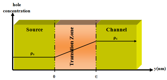
Fig. 7. Diagram of hole injection at around transition zone.
Fig. 7 shows the overlap of two independent distribution functions at the electrode (source)-channel interface. There exist concentration tails along the x-direction characterized by the Debye length of the channel carriers (yc) and that of the source carriers (ys)
So the channel carriers and the source carriers are respectively defined by:
![]() (24)
(24)
![]() (25)
(25)
In this case we can neglect the contribution of yc because ρc >> ρs, yc >>ys so that the transition from ρs to ρc can be simplified to a single exponential function:
![]() (26)
(26)
so the thickness of the trasition (ϵ) zone is given by :
![]() (27)
(27)
à![]() (28)
(28)
from the equation (27)we see better that the thickness on the transition zone varies along the semiconductor thickness if the ρc and ρs change together along the x direction.
![]() (29)
(29)
By putting equation (27) and equation (28), and using ρc>>ρs we obtain:
![]() (30)
(30)
Finally the elemental conductance dGc of the volume element delimited by the channel width (Z), the thickness of the transition zone ϵ and dy:
d![]() (31)
(31)
Consequently the contact resistance Rc is obtained by substituing equation (28) and (30) in (31):
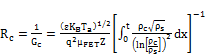 (32)
(32)
3.2.3. Field Effect Mobility
The field effect mobility is calculated from the experimental curves Id = f (Vg). In the linear region the transconductance is given by:
![]() (33)
(33)
so the experimental field mobility is given by :
![]() (34)
(34)
In Fig. 8 we present the variation of field effect mobility as a function of the gate voltage. In Fig. 8 we distinct two different regimes the first at low gate voltage and the second at high voltage. At low gate voltage the field effect mobility varies linearly according the gate voltage. This variation can be adequately described by the gradual filling of trap states as the Fermi level at the semiconductor/insulator interface approaches the transport orbital (HOMO in the case of p-type materials).
This is reasonable because an octithiophene film contains a large number of trapping sites, most of which located at the grain boundaries [27-28].This regime is fitted by the equation (35).
![]() (35)
(35)
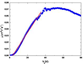
Fig. 8. Measurement field effect mobility as a function of gate voltage. The circle and full line correspond, respectively, to measured data and theoretical model at low Vg.
This equation is given by the multiple trapping and release (MTR) process with an exponential density of states (DOS) near the band edge where Ta is the characteristic temperature and γ is fit constant. The values given a good agreement with the experimental data for the first regime are listed in Table I
Table I. The parameters given by mobility fit.
| Ta (K) | Vth (V) | γ |
| 411 | -2.65 | 12.3E-6 |
For the second regime at high gate voltage the field effect mobility slight decrease by the field induced mobility degradation [29]. It is likely that the mobility near the insulator surface is lower than that at the bulk region due to various surface scattering agents.
When Vg increases, field-induced holes are more concentrated at this low-mobility near-insulator region so that the effective mobility of the conduction path could be reduced [20].
3.2.4. Transfer Line Method (TLM)
The transfer-line method (TLM) also called transmission-line method, or sometimes, transfer-length method, is widely used for organic field-effect transistors OFETs contact resistance evaluation [30-34]. This method was first developed to estimate the contact resistance value of amorphous silicon thin-film transistors [35]. It necessitates several transistors of various channel lengths and provides the average contact resistance value of the whole set of studied transistors. In linear regime, the channel could be approximately regarded as a uniform resistance controlled by the gate voltage. Hence the channel resistance reads![]() , where Z is the channel width, L is the channel length, µ is the mobility, and Cox is the unit area capacitance of the dielectric. Vg and Vth are the gate voltage and threshold voltage, respectively.
, where Z is the channel width, L is the channel length, µ is the mobility, and Cox is the unit area capacitance of the dielectric. Vg and Vth are the gate voltage and threshold voltage, respectively.
Due to the access or contact resistance located between the contacts and the channel, the total resistance Rtot should be complemented by an additional the source drain resistance Rsd, such that the total contact resistances became Rtot =Rc+Rsd. The total resistance is usually normalized by the channel width Z in order to become universal for devices with different channel with Z. Thus we have following:[35]
![]() (36)
(36)
So, in Fig. 9 we plot the variation of the Rtot×Z via a channel length L, at a constant gate voltage Vg. The intercept to the y-axis (i.e. L=0) gives Rsd×Z. At different value of gate voltage Vg, that intercept varies with Vg, thus providing the gate-voltage dependent contact resistance Rsd×Vg[35]. Also the slopes of the linear regression allow us to analyze the gate-voltage dependent mobility Vg [35]. It should be noted that the uncertainty on the slopes of linear regression directly alters the accuracy of subsequently extracted contact resistances.
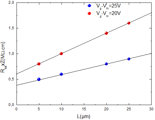
Fig. 9. The overall device resistance via channel length.
3.2.5. Summary
In Fig. 10 we present the variation of the contact resistance as a function of the gate voltage. The stars present the experimental data, the solid lines show the model studied using a constant mobility (in this case the mobility is equal to 0.1 cm2 V-1S-1[36,37] and the circles show the model where the mobility depend to the gate voltage. Fig .10 shows good accord between an experimental data and the theoretical model when the mobility depend to gate voltage. Moreover, this model has allowed us to determine the injection barrier Eb. A good agreement is given for Eb=0.27eV, so gate voltage Vg and injection barrier Eb are the important parameters to command the contact resistance Rc. On the other hand, the second model used is given by substituted the equation of mobility (equation (35)) in the equation of contact resistance (equation (36)). The variation of contact resistance using this model (fig 10 circles) decreases rapidly with increasing gate voltage. Note that the entire curve of mobility given by Fig. 8 cannot be modeled by a simple analytical expression, so we only took the trap-dominated regime (linear regime) for the analysis in Fig. 9.
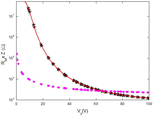
Fig. 10. The overall device resistance via gate voltage. The stars according to the experimental data, solid line according to theoretical model for Vg mobility depend and circle according to model where field effect mobility is constant.
4. Conclusion
At present, a theoretical model for a polythiophene thin film transistor is detailed by solving the Poisson equation and using an analytical approximation for the charge distribution model inside an organic semiconductor. From this model an equation of a contact resistance was proposed .The dependence of the contact resistance and the gate voltage was explained. Using this model two cases are treated. First, the contact resistance is calculated with a constant mobility of 0.1 cm2V-1 S-1. This model cannot reproduce the experimental data. Second, the contact resistance is calculated mobility depend to gate voltage. A good agreement between experimental data is given. The injection barrier Eb at the interface Au/ Polythiophene is estimated. From the classical theory of metal/insulator contact the equation of the charge distribution was determined.
Acknowledgement
This work was supported by grants from the Tunisian Ministry of Higher Education.
References
- A. Tsumura, H. Koezuka, T. Ando, Appl.Phys. Lett. 49, 1210 (1986)
- Y.Y. Lin, D.J. Gundlach, S.F. Nelson, T.N. Jackson, IEEE Electron Device Lett. 18, 606 (1997)
- G. Horowitz, R. Hajlaoui, R. Bourguiga, M. Hajlaoui, Synth. Met. 101, 401 (1999)
- Z. Bao, A.J. Lovinger, A. Dodabalapur, Appl. Phys. Lett. 69, 3066 (1996)
- Z.A. Bao, A.J. Lovinger, J. Brown, J. Am. Chem. Soc. 120, 207 (1998)
- D. Shukla, S.F. Nelson, D.C. Freeman, M. Rajeswaran, W.G. Ahearn, D.M. Meyer, J.T. Carey, Chem. Mater. 20, 7486 (2008)
- H. Sirringhaus, P.J. Brown, R.H. Friend, M.M. Nielsen, K. Bechgaard, B.M.W. Langeveld-Voss, A.J.H. Spiering, R.A.J. Janssen, E.W. Meijer, P. Herwig, D.M. de Leeuw, Nature 401, 685 (1999)
- P.F. Baude, D.A. Ender, M.A. Haase, T.W. Kelley, D.V. Muyres, S.D. Theiss, Appl. Phys. Lett. 82, 3964 (2003)
- R. Rotzoll, S. Mohapatra, V. Olariu, R. Wenz, M. Grigas, K. Dimmler, O. Shchekin, A. Dodabalapur, Appl. Phys. Lett. 88, 123502 (2006)
- H.E.A. Huitema, G.H. Gelinck, J. van der Putten, K.E. Kuijk, C.M. Hart, E. Cantatore, P.T. Herwig, A. van Breemen, D.M. de Leeuw, Nature 414, 599 (2001)
- G.H. Gelinck, H.E.A. Huitema, E. van Veenendaal E. Cantatore, L. Schrijnemakers, J. van der Putten, T.C.T. Geuns, M. Beenhakkers, J.B. Giesbers, B.H. Huisman, E.J. Meijer, E.M. Benito, F.J. Touwslager, A.W. Marsman, B.J.E. van Rens, D.M. De Leeuw, Nat. Mater. 3, 106 (2004)
- J.A. Rogers, Z. Bao, K. Baldwin, A. Dodabalapur, B. Crone, V.R. Raju, V. Kuck, H. Katz, K. Amundson, J.Ewing, P. Drzaic, Proc. Natl. Acad. Sci. USA 98, 4835 (2001)
- B. Comiskey, J.D. Albert, H. Yoshizawa, J. Jacobson, Nature 394, 253 (1998)
- M. Shur, M. Hack, J. Appl. Phys. 55 (1984) 3831.
- Y.Y. Lin, D.J. Gundlach, T.N. Jackson, S.F. Nelson, IEEE Trans. Dev. 44 (1997) 1325.
- G. Horowitz, Adv. Mater. 10 (1998) 365
- S. Zorai and R. Bourguiga, Eur. Phys. J. Appl. Phys. 59 (2012) 20201.
- S. Mansouri, M. Mahdouani, A. Oudir, S. Zorai, S. Ben Dkhil, G. Horowitz, R. Bourguiga, Eur.Phys. J. Appl. Phys. 48 (2009) 30401.
- S. Zorai, S. Mansouri and R. Bourguiga, Superlattices and Microstructures 52 (2012) 1103–1118.
- G. Horowitz, J. Mater. Res. 19 (2004) 1946.
- P.V. Necliudov, M.S. Shur, D.J. Gundlach, T.N. Jackson,J. Appl. Phys. 88, 6594 (2000)
- G. Horowitz, R. Hajlaoui, P. Delannoy, J. Phys. III France 5, 1786 (1995)
- W.E. Spear, P.G. Le Comber, J. Non-Cryst. Solids 727, 8 (1972)
- C. H. Kim, Y. Bonnassieux, G. Horowitz.IEEE Trans. Electron Devices, , 60 (2013), 280.
- S. M. Skinner, J. Appl. Phys., 26, (1955) 5, 498–508
- S. M. Sze and K. K. Ng, Physics of Semiconductor Devices, 3rd ed. New York: Wiley, 2007.
- S. Verlaak, V. Arkhipov, and P. Heremans.,82( 2003) 745–747.
- A. Bolognesi, M. Berliocchi, M. Manenti, A. D. Carlo, P. Lugli, K. Lmimouni, and C. Dufour, IEEE Trans.Electron Devices, 51 (2004)1997–2003.
- M. Mottaghi and G. Horowitz, Org. Electron., 7,(2006) 528–536.
- J. Zaumseil, K. W. Baldwin, and J. A. Rogers, J. Appl. Phys. 93, (2003) 6117
- P. V. Necliudov, M. S. Shur, D. J. Gundlach, and T. N. Jackson, Solid-State Electron. 47, (2003).259
- H. Klauk, G. Schmid, W. Radlik, W. Weber, L. S. Zhou, C. D. Sheraw, J. A. Nichols, and T. N. Jackson, Solid-State Electron. 47, (2003) 297.
- D. J. Gundlach, L. Zhou, J. A. Nichols, T. N. Jackson, P. V. Necliudov, and M. S. Shur, J. Appl. Phys. 100, (2006).024509
- T. Minari, T. Miyadera, K. Tsukagoshi, Y. Aoyagi, and H. Ito, Appl.Phys. Lett. 91, (2007) 053508
- S. W. Luan and G. W. Neudeck, J. Appl. Phys. 72, (1992) 766.
- S. Zorai, S. Mansouri, R. Bourguiga Superlattices and Microstructures 55 (2013) 211–221.
- S. Mansouri, S. Zorai and R. Bourguiga,Synthetic Metals162 (2012) 231–235


