
International Journal of Modern Physics and Applications, Vol. 1, No. 3, July 2015 Publish Date: Jul. 10, 2015 Pages: 99-105
Characterization of P-Type Zinc Oxynitride Thin Films Prepared by MOCVD Using Bis (Glycinato-N, O) Zinc Precursor
U. S. Mbamara1, *, A. I. Akinwande2, I. A. O. Ojo3, E. O. B. Ajayi4
1Department of Physics, Federal University of Technology, Owerri, Nigeria
2Department of Electrical Engineering and Computer Science, Massachusetts Institute of Technology, Cambridge, USA
3Department of Chemistry, Obafemi Awolowo University, Ile-Ife, Nigeria
4Department of Physics, Obafemi Awolowo University, Ile-Ife, Nigeria
Abstract
A novel precursor complex, the bis (glycinato-N, O) zinc, was synthesized and used to deposit zinc oxynitride thin films on SiO2 substrates at 390°C and 420°C respectively, by metalorganic chemical vapour deposition (MOCVD) technique. The thin films produced were characterized with hot probe, x-ray diffractometry (XRD), x-ray photoelectron spectroscopy (XPS) and dynamic secondary ion mass spectroscopy (SIMS). The hot probe tests showed that the thin films had p-type conductivity. XRD spectra of the films gave poorly defined peaks, signifying blurred crystallinity. The XPS analyses revealed the presence of Zn, O and N peaks, with the thin films deposited at 390°C having higher N-doping level than those deposited at 420°C. Results of dynamic SIMS tests by destructive layer analyses of the films were inconclusive. The thin films were very thin, and the results indicate that lower deposition temperatures using the new precursor may be preferred to higher temperatures. Applications of the p-type zinc oxynitride are possible in optical and solid state electronics.
Keywords
Precursor, Bis (Glycinato-N, O) Zinc, MOCVD, Thin Films, P-type Zinc Oxynitride
Received:June 2, 2015
Accepted: June 10, 2015
Published online: July 9, 2015
@ 2015 The Authors. Published by American Institute of Science. This Open Access article is under the CC BY-NC license. http://creativecommons.org/licenses/by-nc/4.0/
1. Introduction
Zinc oxide thin film has become a handy material for several solid state applications due to its many favourable properties. Such properties include high optical transparency, wide bandgap of about 3.4 eV, large exciton binging energy of 60 meV, high crystallinity, hexagonal wurtzite structure, high chemical and thermal stability, ease of handling and fabrication and high piezoelectric coefficient. Various electronic and optoelectronic devices which exploit these properties are already in use [1-4]. There are also now the added discovery of applicability in surface acoustic wave devices and high electromechanical coupling coefficient suitable for applications in nanoelectromechanical (NEM) and microelectromechanical (MEM) devices [5,6]. Different techniques including physical, chemical and sputtering methods and their combinations have variously been used in depositing the thin films. The method of deposition plays a significant role in determining which of the highlighted properties predominates in the deposited thin film.
Zinc oxide as a key semiconductor element is native n-type, and realizing a p-type version of the material is an up-hill task because of the asymmetric nature of its lattice structure. The possibility is there, however, and among several options the N atom is believed to be a very suitable substitute for O in the lattice to effect a significant p-type doping. We have previously used the metalorganic chemical vapour deposition (MOCVD) method to realize N-doping, by adopting a special precursor combination technique [7]. The result was saturated N-combinations with the ZnO as was reported. The desire to achieve minority N-doping which will furnish an effective p-type material led to the consideration of a different single solid source precursor complex, the bis(glycinato-N,O) zinc, or glycine zinc complex, to deposit a zinc oxynitride or N-doped ZnO thin films, by metalorganic chemical vapour deposition (MOCVD) technique. This is what this work was set to achieve.
2. Methods
The precursor used was prepared with zinc chloride, 2-aminoacetic acid (glycine) and sodium hydroxide. Stoichiometric amounts of the three substances were reacted according to the equation
ZnCl2 + 2C2H5O2N + 2NaOH → C4H8N2O4Zn + 2NaCl + 2H2O
The bis (glycinato-N, O) zinc or glycine zinc complex (C4H8N2O4Zn) was thereafter separated and dried for use as a single solid source precursor for the work. Its structural formula is of the form.
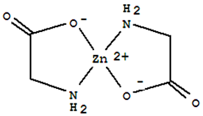
Figure 1. Bis (glycinato-N, O) zinc structure.
The precursor was placed in the receptacle of metalorganic chemical vapour deposition (MOCVD) unit, and its vapour was passed through the cracking chamber of the unit to deposit the zinc oxynitride thin film. Oxidized silicon wafers (SiO2) were used as the substrates while the flow rate of the precursor vapour was maintained at 2.5 dm3m-1, with air as the carrier gas. Two different sets of deposition were carried out, one at 390°C, and the other at 420°C, for two hours each at atmospheric pressure. The thin films emanating from the depositions were respectively labeled as Sample A and Sample B.
The samples were characterized by using Hot Probe, X-Ray Diffractometry (XRD), X-ray Photoelectron Spectroscopy (XPS) and Dynamic Secondary Ion Mass Spectroscopy (SIMS). The Hot probe was done by placing two droplets of silver paste side by side each other about 1 mm apart on the surface of the test sample. Then the cold electrode was placed on one of the drops at room temperature while the hot probe (soldering iron) was set to be placed on the other drop, without letting the two probes touch each other. The probe terminals were connected through a nanocurrent amplifier to a null deflection microammeter. As soon as the hot probe was placed on the silver drop, the meter was monitored for deflection to the left (indicating n-type) or the right (indicating p-type). An uncoated substrate and samples A and B were tested for carrier types using this technique.
In the XRD analyses the samples A and B were scanned through 2θ = 20° to 65°. Also scanned was a sputtered 15nm ZnO thin film on Si substrate (MIT test standard) to act as comparison. The XPS examination of samples A and B were carried out along with the sputtered 15nm ZnO thin film. The XPS charts were correlated with standards and the doping levels of samples A and B compared. The dynamic SIMS analyses were done on samples A and B by destructive layer by layer analyses for elemental compositions and stoichiometry.
3. Results and Discussions
In the hot probe examination, the uncoated SiO2 substrate gave deflection to the left, indicating n-type conductivity, while the coated samples A and B gave deflections to the right, each indicating p-type conductivity. These results show that p-doping was realized in the thin films. The deflection due to sample A was greater than that due to sample B. After a comprehensive investigation and confirmation of these p-type doping results through the MOCVD method, and using the glycine zinc precursor, it will become possible to build whole solid state devices and touch-sensitive display panels using zinc oxide alone, say by applying the undoped material for the n-type, and the N-doped material for the p-type.
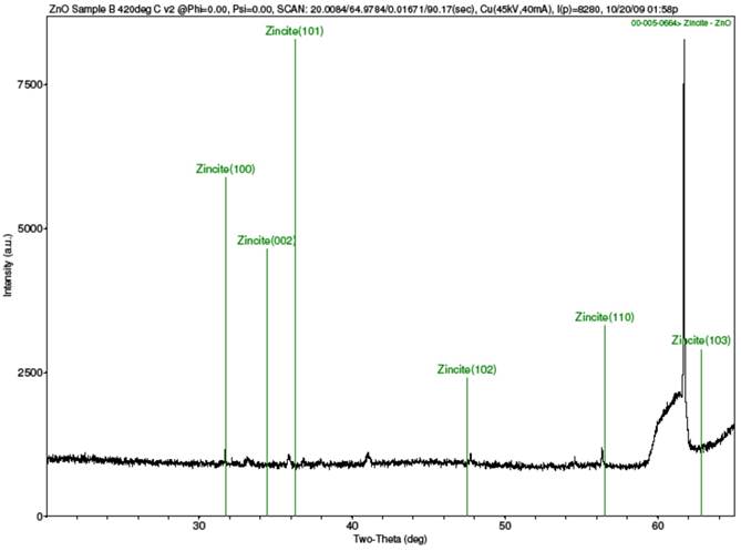
Strong peaks were not obtained from the XRD scans of the samples, as the results in Fig. 2 show. Figure 2(a) is for sample A, Fig. 2(b) is for sample B, Fig. 2(c) is the combined spectra of samples A and B, and Fig. 2(d) is the spectrum for the MIT standard ZnO test sample. The results of the samples A and B did closely match each other, as can be seen from the combined Fig. 2(c) When compared with the XRD result for the MIT standard in Fig 2(d), one can testify that though the peaks for the samples were stunted, they did occur similarly as for the standard peaks, save for slight shifts in their 2θ angles. The stunted appearance of the sample peaks is strongly believed to be as a result of the films being too thin, or from the calibration of the XRD machine, the latter possibility being plausible if one considers the fact that the peaks for the MIT test standard, though better defined than for samples A and B, are equally not prominently sharp.
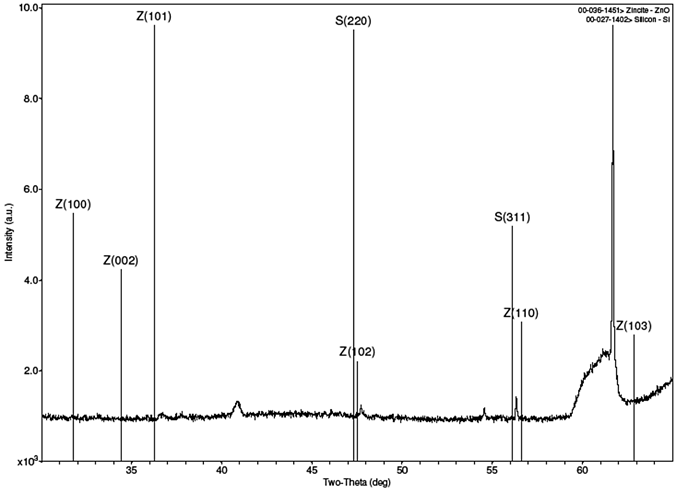
(a) XRD spectrum for sample A with ZnO library peaks overlay.
(b) XRD spectrum for sample B with ZnO library peaks overlay.
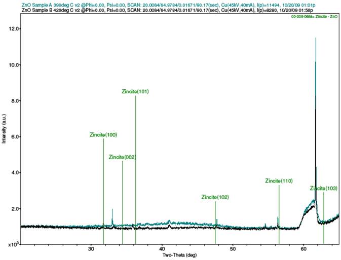
(c) Combined XRD spectra of samples A and B with ZnO library peaks overlay: Teal-Sample A; Black- Sample B.
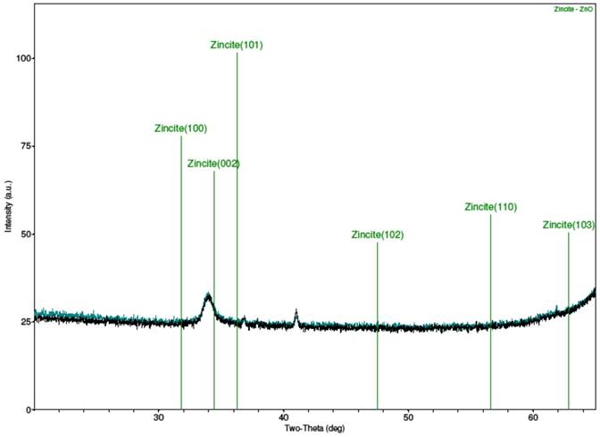
(d) XRD spectrum of sputtered 15 nm thick ZnO thin film on Si substrate (MIT test standard).
Figure 2. XRD spectra of samples A and B and MIT standard ZnO test sample.
Also, some workers had previously reported poor crystallinity of their ZnO thin films and attributed it to different reasons [8-10], but one significant tally with the present work is that of Tan et al [11], in which diminished crystallinity was attributed to the introduction of a N-dopant to realize p-type conductivity. So the diminution of prominent peaks in these XRD results is also attributable to the p-type nature of the thin films.
In Fig. 3 are displayed the XPS spectra of the thin films. Figure 3(a) contains the spectra of samples A and B, Fig. 3(b) is the combined spectra of samples A and B and the MIT test standard, Fig. 3(c) and Fig. 3(d) are portions of the spectra for samples A and B, rescanned at 2 eV to respectively highlight the Zn 2p peaks and the N 1s peaks. The XPS spectra of samples A and B in Fig. 3(a) are seen to match each other, and reveal the presence of the key elements, viz, Zn, O and N. In Fig. 3(b) the samples spectra perfectly match the spectrum of the MIT test standard sample with respect to the elemental peaks, save for their relative intensities which are less prominent for samples A and B.
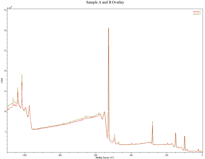
(a) Combined XPS spectra of samples A and B: Red – Sample A; Green – Sample B.
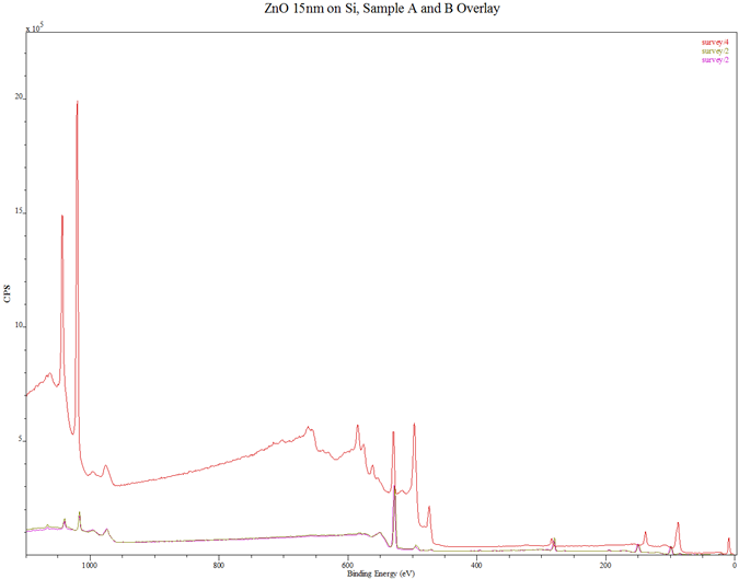
(b) Combined spectra of samples A, B and MIT test standard for comparison: Green – Sample A; Blue – Sample B; Red – MIT test standard.
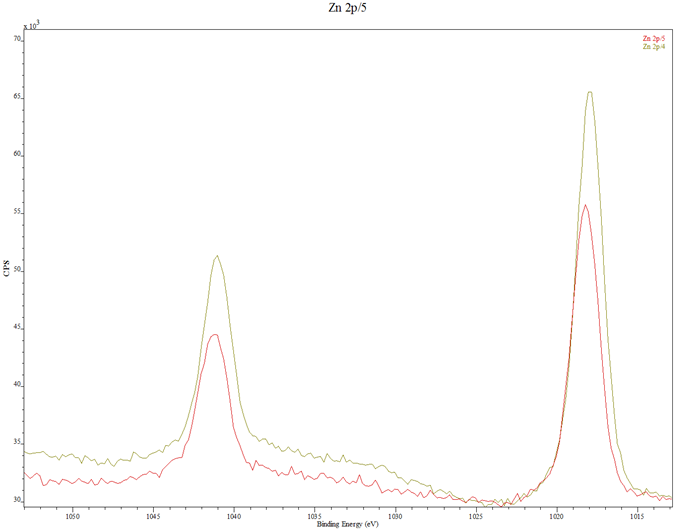
(c) Zn 2p peaks of samples A and B rescanned at 0.2eV per step for higher resolution and comparison: Red – Sample A; Green – Sample B.
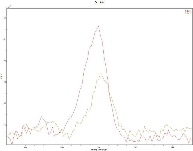
(d) N 1s peaks for samples A and B, rescanned at 0.2 eV per step for higher resolution and comparison: Red – Sample A; Green – Sample B.
Figure 3. XPS spectra of samples A and B and the MIT test standard sample.
Compared with the 15 nm thick standard sample, the dwarfed intensities of samples A and B indicate that the coatings were very thin, possibly less than 5 nm thick. Some stray elements (Na, Cl, C and K) were also detected. They may have originated from the substrates cleaning process or wrong handling. The O peaks are sufficiently prominent in the spectra. The rescanned spectra of Fig. 3(c) and Fig. 3(d) show that while the Zn level in sample B is higher than that in sample A, the N-doping level in sample A is higher than that in sample B. This latter development may be the reason behind sample A having higher current flow than sample B in the hot probe tests.
Looking back at the samples deposition parameters, it seems quite cogent that the lower deposition temperature of sample A (390°C) as against that of sample B (420°C) allowed the ZnO matrixes in sample A to accommodate more N atoms than those of sample B. Lower deposition temperatures, down to about 300°C, are hence advocated in future work with the bis (glycinato-N, O) zinc precursor (boiling point = 250°C). Perfecting the production sets the stage for cheap electronics using the doped and undoped ZnO materials for components.
Dynamic SIMS analyses were carried out on samples A and B by destructive layer analysis to establish the compositions and stoichiometry of the elements present. Because of the very low thinness of the thin films however, no conclusive results were obtained from the SIMS analyses.
4. Conclusion
This work utilized a novel precursor, the bis (glycinato-N, O) zinc or glycine zinc complex to deposit p-type zinc oxynitride thin films by metalorganic chemical vapour deposition (MOCVD) technique. The thin films obtained were very thin, possibly less than 5nm thick. XRD scans gave spectra with poor crystallinity due to the p-type nature and small thickness of the films. XPS spectra showed that films deposited at 390°C had higher doping level than films deposited at 420°C, indicating that lower deposition temperature may be preferable for higher doping levels and thicker films. Dynamic SIMS analyses of the samples were inconclusive owing to very low thinness of the thin films. Applications of the new materials are possible in transparent and solid state electronics.
Acknowledgements
Our gratitude goes to the following: Department of Physics, Obafemi Awolowo University, Ile-Ife, Nigeria, for allowing the use of their MOCVD facilities and hot probe set up; Department of Electrical Engineering and Computer Science, Massachusetts Institute of Technology, Cambridge, USA, for XRD and XPS analyses; Evans Analytical Group (EAG) for SIMS analyses; Department of Physics, Federal University of Technology, Owerri, Nigeria, for their general support.
References
- Y. Lu, Z. Ye, Y. Zeng, W. Xu, L. Zhu and B. Zhao. Effects of RF power variation on properties of N-doped p-type ZnO thin films grown by plasma-assisted MOCVD. Optical Materials 29 (2007) 1612–1615. doi:10.1016/j.optmat.2006.08.004.
- V. Snitka, V. Jankauskas, A. Zunda and V. Mizariene. Deposition of nanocrystalline ZnO by wire explosion technique and characterization of the films' properties. Materials Letters 61 (2007) 1763–1766. doi:10.1016/j.matlet.2006.07.189.
- D. Scarano, S. Bertarione, F. Cesano, J.G. Vitillo and A. Zecchina. Plate-like zinc oxide microcrystals: Synthesis and characterization of a material active toward hydrogen adsorption. Catalysis Today 116 (2006) 433–438. doi:10.1016/j.cattod.2006.05.062.
- W.L. Dang, Y.Q. Fu, J.K. Luo, A.J. Flewitt and W.I. Milne. Deposition and characterization of sputtered ZnO films. Superlattices and Microstructures (2007) 1-5, doi:10.1016/j.spmi.2007.04.081.
- M. Hamida, A.A. Tahir, M. Mazhar, F. Ahmad, K.C. Molloy and G. Kociok-Kohn. Deposition and characterization of ZnO thin films from a novel hexanuclear zinc precursor. Inorganica Chimica Acta xxx (2007) 1-7. doi:10.1016/j.ica.2007.07.013.
- E. C-etino¨rgu¨, S. Goldsmith and R.L. Boxman. The effect of substrate temperature on filtered vacuum arc deposited zinc oxide and tin oxide thin films. Journal of Crystal Growth 299 (2007) 259–267. doi:10.1016/j.jcrysgro.2006.11.334.
- U. S. Mbamara, O. O. Akinwunmi, E. I. Obiajunwa, I. A. O. Ojo, E. O. B. Ajayi. Deposition and Characterisation of Nitrogen-Doped Zinc Oxide Thin Films by MOCVD Using Zinc Acetate—Ammonium Acetate Precursor, Journal of Modern Physics, 3 (2012). 652-659. doi:10.4236/jmp.2012.38089.
- E. Fortunato, P. Barquinha, A. Pimentel, A. Gonçalves, L. Pereira, A. Marques and R. Martins. Next Generation of Thin Film Transistors Based on Zinc Oxide. Mat. Res. Soc. Symp. Proc. 811 (2004). 1-6.
- S. T. Tan, B. J. Chen, X. W. Sun, W. J. Fan, H. S. Kwok, X. H. Zhang and S. J. Chua. Blueshift of optical band gap in ZnO thin films grown by metal-organic chemical-vapor deposition. Journal of Applied Physics 98 (013505) 2005. 1-5. doi: 10.1063/1.1940137.
- S. O'Brien, M.G. Nolan, M. Çopuroglu, J.A. Hamilton, I. Povey, L. Pereira, R. Martins, E. Fortunato and M. Pemble. Zinc oxide thinfilms: Characterization and potential applications. Thin Solid Films 518 (2010). 4515–4519. doi:10.1016/j.tsf.2009.12.020.
- S.T. Tan, B.J. Chen, X.W. Sun, M.B. Yu, X.H. Zhang and S.J. Chua. Realization of Intrinsic p-Type ZnO Thin Films by Metal organic chemical vapor deposition. Journal of Electronic Materials 34(8). 2005. 1172-1176.


