
Journal of Nanoscience and Nanoengineering, Vol. 1, No. 4, December 2015 Publish Date: Sep. 18, 2015 Pages: 193-197
Absorbance Spectra of CdS Thin Film at Varying Concentration of Ligand
I. A. Ezenwa*, C. I. Elekalachi
Department of Industrial Physics, Chukwuemwka Odumegwu Ojukwu University, Anambra State, Nigeria
Abstract
Cadmium sulphide (CdS) thin films was deposited by chemical bath method onto glass substrate at room temperature. The absorbance spectra of the fabricated films were obtained with a Janway 6405 UV / Visible spectrophotometer in the wavelength range of 200nm - 1100nm. Structural and surface morphology of the films were carried out using an x-ray diffractometer with Cuk α radiation and Olumpus Optical microscope. Absorbance spectra of CdS thin film fabricated at varying concentration of ligand show very high absorbance in the UV region, moderate absorbance in the VIS region and relatively low absorbance in the NIR. There was no clear cut effect of the varying concentration of ligand on the absorbance of the deposited films.
Keywords
Cadmium Sulphide, Chemical Bath Deposition, Ligand, Absorbance Spectra
Received: August 22, 2015
Accepted: September 2, 2015
Published online: September 17, 2015
@ 2015 The Authors. Published by American Institute of Science. This Open Access article is under the CC BY-NC license. http://creativecommons.org/licenses/by-nc/4.0/
1. Introduction
CdS thin films have properties that are suitable for solar cell fabrication. They have good optical transmittance, a wide bandgap and good electrical properties. CdS thin films also have high absorption coefficient, electron affinity and easy ohmic contact, making them suitable for solar cell application. It is used as a window electrode because of its stability and reasonable conversion efficiency. The conductivity of CdS increases when irradiated with light [1] leading to it use as a photoresistor.When combined with a p - type semiconductor, it forms the core component of a photovoltaic cell [2]. When doped with for example Cu2+ and Al3+, CdS luminescence and is used as phosphors [3]. CdS crystal can act as a solid state laser [4]. It is also one of the first semiconductor material to be used for thin film transistor [5]. Thin films of CdS can be piezoelectric and have been used as transducers. CdS thin films have widely been grown by researchers using chemical bath method because it is a more simple technique that produces quality films, [6], [7] [8] and [9] grew CdS thin films using chemical bath technique.
This work present the fabrication of CdS thin film using chemical bath method and the analysis of the absorbance spectra at wavelength range of 200 - 1100nm. The effect of the concentration of ligand on the absorbance of the fabricated films was also looked at.
2. Materials and Methods
Chemical bath method was employed for the deposition of CdS thin film. The reaction bath for the deposition of cadmium sulphidewas composed of cadmium bromide (CdBr2), thiourea, triethanolamine (TEA) and ammonia solution. CdBr2 was used as cadmium ion source, while thioureawas used as sulphide ion source. TEA was used as our ligand and ammonia solution was used for pH adjustment.
In this experiment, five reaction baths (50mls beaker) were used. 5mls of CdBr2 was measured into a 50ml beaker and various volumes of TEA were then added as indicated in Table 1. 5mls of thiourea solution was added, followed by 5mls of ammonia solution. Each bath was topped to 50mlsmark by adding distilled water and stirred to ensure uniformity of the mixture. Glass slides were then dipped vertically into the baths and left to stand for four hours, after which they were removed and dried in air.Theexperiment was conducted at room temperature. Janway 6405 UV/visible spectrophotometer was used to determine the spectra absorbance. Structural and surface characterization of the films was carried out using an x-ray diffractometer with Cukα radiation and Olumpus optical microscope respectively. Other solid state and optical properties of the films had been investigated in our earlier publication [10].
Table 1. Bath constituents for the chemical bath deposition ofCdS thin film.
The reaction mechanism is of the form:
CdBr2.4H2O + TEA ![]() Cd [TEA]2++ 2HBr +3H2O
Cd [TEA]2++ 2HBr +3H2O
Cd [TEA]2+![]() Cd2++ TEA
Cd2++ TEA
(NH2)2 CS + OH-![]() CH2N2 + H2O + HS-
CH2N2 + H2O + HS-
HS- + OH-![]() H2O + S2-
H2O + S2-
Cd2++ S2-![]() CdS
CdS
3. Results and Discussion
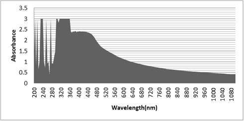
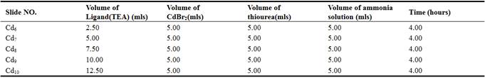
Fig. 1. Graph of absorbance versus wavelength at 2.5mls volume of ligand.
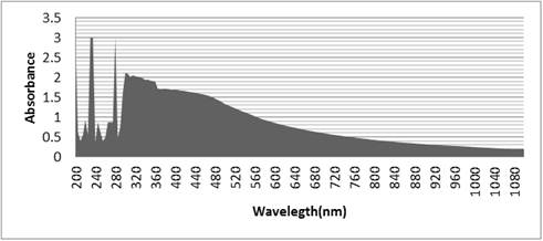
Fig. 2. Graph of absorbance versus wavelength at 5mls volume of ligand.
Fig. 3. Graph of absorbance versus wavelength at 7.5mls volume of ligand.
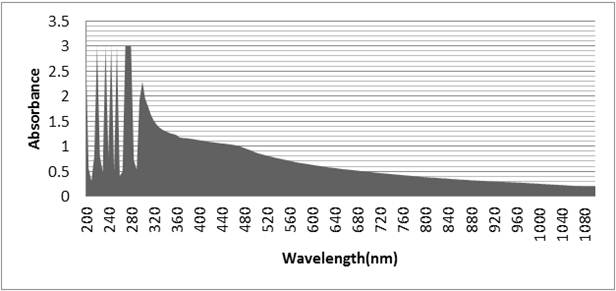
Fig. 4. Graph of absorbance versus wavelength at 10mls volume of ligand.
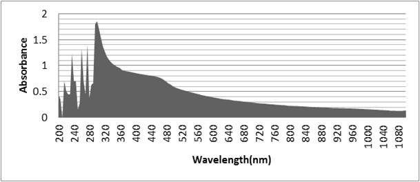
Fig. 5. Graph of absorbance versus wavelength at 12.5mls volume of ligand.
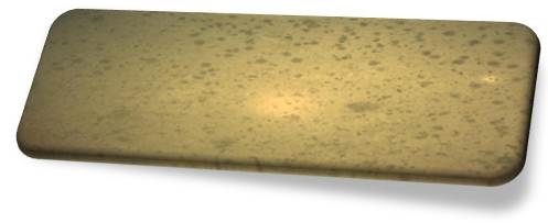
Fig. 6. Micrographs of CdS thin film.
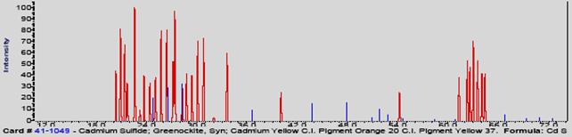
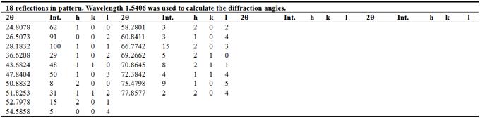
Fig. 7. X-ray diffraction spectra for deposited CdS thin film.
Table 2. X-ray result of deposited CdS thin film.
Looking at the absorbance spectra of the deposited films, it will be seen that the absorbance was highest in the UV region of the electromagnetic spectrum, with the highest peak in the range of 200 - 350nm for Fig. 1, for Fig. 2, the highest peak was noticed at 250nm and 300nm. For Fig. 3, the highest peak was observed at 250nm, while for Fig. 4 and 5, the peaks were noticed at wavelength range of 220 - 270nm and 300nm respectively.
In the visible region, there were no pronounced peaks, but the absorbance gradually decreased throughout the visible region of the electromagnetic spectrum. The highest absorbance for Fig. 1 was at a wavelength range of 400 - 500nm and 400 - 430 for Fig.2. Fig. 3 has the highest peak at 460nm. For Fig. 4 and 5, the highest absorbance was at 450nm.
In the near infrared region (NIR), the absorbance was relatively generally low. All the samples have almost the same absorbance value of ![]() at the NIR of the spectrum. Therefore, it can be inferred that the absorbance of CdS thin film fabricated at varying concentration of ligand show very high absorbance in the UV region, moderate absorbance in the VIS region and relatively low absorbance in the NIR. This property makes CdS thin film useful in applications such as protective coating. Also, critically looking at the absorbance spectra, it will be seen that there is no clearcut effect of the varying concentration of ligand on the absorbance of the deposited films.
at the NIR of the spectrum. Therefore, it can be inferred that the absorbance of CdS thin film fabricated at varying concentration of ligand show very high absorbance in the UV region, moderate absorbance in the VIS region and relatively low absorbance in the NIR. This property makes CdS thin film useful in applications such as protective coating. Also, critically looking at the absorbance spectra, it will be seen that there is no clearcut effect of the varying concentration of ligand on the absorbance of the deposited films.
Figure 6 shows the optical micrograph of our deposited CdS thin film. From the micrograph, it is evident that the surface of the film is smooth and covers the glass substrate well. The grains are very small with unequal size and shape.
According to the XRD results, the chemically deposited films of CdS are of cubic structure. This crystal structure is consistent with [11]. From the XRD measurements, a lattice constant of 5.6954Ǻ was calculated for CdS thin film in the (101) plane at a maximum intensity of 2q = 28.183 using Bragg’s law given by n = 2dsinq.
4. Conclusion
We have fabricated CdS thin film using chemical bath deposition technique.Absorbance data of the films were obtained using a Janway 6405 UV/Visible spectrophotometer. Structural and surface morphology of the films were carried out using an x-ray diffractometer with Cukα radiation and Olumpus Optical microscope. Absorbance spectra of CdS thin film fabricated at varying concentration of ligand show very high absorbance in the UV region, moderate absorbance in the VIS region and relatively low absorbance in the NIR.There was no clear cut effect of the varying concentration of ligand on the absorbance of the deposited films.
References
- D. Lincot and Gary Hodes, Chemical solution deposition of semiconducting and non metallic films. Proceeding of the International symposium, the Electrochemical Society, (2006).
- Antonio Luque, SterenHegedus,Hand book of photovoltaic science and engineering, John Willy and sons, (2003).
- C. Fouassier, Lumine science in Encyclopidia of Inorganic Chemistry, John Wily and Sons, (1994).
- Agarwal, Ritesh, Barrelet, carl j., Liebier, Charles M., Lasing in single cadmium sulphide nanowire optical cavity, Nano Letters, 5(5), pp. 917 - 920, (2005).
- P. K. Weimer, The TFT, a new thin film transistor, Proc. IRE, Vol. 50, No. 6, pp. 1462 - 1469, (1962).
- J. G. Vazquez-Luna, R. B. Lopez Flores, M. Rubin-Falfan, L. Del C. Gomez - pavon, R Lozada-morals, H. Jurez-santiesteban, O. Starostenko, O Zelaya-Angel, O. Vigil, and A. Gonzalez, CdS thin film deposited by modified chemical bath deposition method. Jour. of Crystal Growth, Vol. 187(3), PP. 380 - 386 (1999).
- J. M. Dora and J. Herrero, Chemical bath deposition of CdS thin films: An approach to the chemical mechanism through the study of the film microstructure, Jour. Electrochem. Soc., 144(11), (1997).
- H. Moualkia, S. Hariech, M. S. Aida, N. Attaf and El Laifa, Growthg and physical properties of CdS thin films prepared by chemical bath deposition. Jour. Phy. D; Applied Physics, Vol. 42(13), (2009).
- Ezenwa I.A., Optical Analysis of Chemical bath Fabricated Cuo Thin Films, Res. J. Recent Sci, Vol. 1(1), pp.46-50, (2012).
- Ezenwa I. A. and Ekpunobi A. J. Deposition and characterization of CdSthin film by chemical bath method, Pacific Journal of Science and Technology, Vol. 11, No. 2, (2010), p p. 435-440.
- Abdullah M. A., Al - Hussam, Salah Abdul –JabbaJassim, Synthesis, structure and optical properties of CdS thin films nanoparticles prepared by chemical bath technique. Jour. of Association of Arab Universities for Basic and Applied Sciences, Vol. 11(1), (2012), pp. 27 - 31.


