
Journal of Nanoscience and Nanoengineering, Vol. 1, No. 3, October 2015 Publish Date: Sep. 1, 2015 Pages: 162-170
Effect of Fractal Parameters on Response of Nanobeam: A Finite Element Approach
D. Dutta1, S. Bhattacharyya2, S. Sahoo3, *
1Department of Mechanical Engineering, M. S. Institute of Technology, Kolkata, India
2Department of Aerospace Engineering, IIST, Thiruvananthapuram, Kerala, India
3Department of Civil Engineering, Heritage Institute of Technology, Kolkata, India
Abstract
Finite element analysis facilitates optimal design of MEMS/NEMS devices for reliability. The same is used here to analyze the effect of types of fractal rough surfaces on static response of nanobeams Three-dimensional rough surfaces are generated using modified two variable Weierstrass-Mandelbrot function with given fractal parameters. Beam with various fractal roughness are modelled to observe the variations in the bending stresses and displacements. The results of the analysis will be useful to designers to develop the most suitable geometry for nanostructures.
Keywords
Nanobeam, Roughness, Fractal, Finite Element Method
Received: August 9, 2015
Accepted: August 24, 2015
Published online: September 2, 2015
@ 2015 The Authors. Published by American Institute of Science. This Open Access article is under the CC BY-NC license. http://creativecommons.org/licenses/by-nc/4.0/
1. Introduction
A large variety of micro/nano-electro-mechanical systems (MEMS/NEMS) are produced using lithographic and other fabrication techniques. Some of the industrial applications of these include digital light products (DLP) devices for digital projection displays, capacitive-type silicon accelerometers for automotive sensory applications, and many more other sensors and actuators. Friction/stiction and wear limit the lifetimes and compromise the performance and reliability of these devices involving relative motion [1]. Structural integrity is of paramount importance in all these devices. Load applied during the use of devices can result in component failure. Cracks can develop and propagate under tensile stresses leading to failure [2]. Stress and deformation analyses are carried out foran optimal design. In general MEMS/NEMS applications need extreme reliability. Recent developments in science and engineering have advanced capability to fabricate and control structures on the scale of micro/nanometers, and have brought problems of material behavior on the micro/nanometer scale into the domain of engineering. Reliability studies are the key for practical applications and commercialization of today’s advanced MEMS/NEMS systems. Many current and potential applications for MEMS/NEMS are not really practical, because their mechanical properties have not been established [3-5].
It is essential for designers of MEMS/NEMS devices to have mechanical property information at the nanoscale as most mechanical properties are known to exhibit a dependence on specimen size. Single-crystal silicon and silicon-based materials are the most common materials used in MEMS. An early study showed silicon to be mechanically resilient material in addition to its favorable electronic properties [6]. Researchers have conducted tests to evaluate mechanical properties of silicon and silicon-based small scale structures including tensile tests and bending tests [7-10]. Recently researchers have used atomic force microscopy-based techniques to fabricate Si-based nanoscale structures and evaluate their mechanical properties [11].
Analytical models can be used for simple geometries and boundary conditions. Numerical models are needed for analysis of complex geometries. Finite element methods (FEM) can be used down to few tens of nanometer scale. FEM has been used for simulation and prediction of residual stresses and strains induced in MEMS devices during fabrication [12]. Finite element analysis has been used to study the effect of geometric variations on the resonance frequency and spring constant of microscale cantilever sensors [13]. FEM based software has been developed to perform fault analysis in order to study MEMS faulty behavior [14]. FEM analysis has been used to compute mechanical strain resulting from doping of silicon [15] and analyze micromechanical experimental data [16] and nanomechanical experimental data [17]. Stress and deformation analyses of nanostructures have been carried out using FEM analysis [18]. However, there are few reports that attempt to consider the finite element analysis of fractal surfaces. One such study [19] considers finite element analysis of non-adhesive, frictionless elastic/elastic–plastic contact between a rigid flat plane and a self-affine fractal rough surface using the commercial finite element package ANSYS. The purpose of this research is to perform stress analysis of nanobeams to study the effect of various fractal roughness parameters on tensile stresses which are responsible for crack propagation.
2. Surface Modelling
Rough surface topographies areexpressed in terms of the height variance, slope and curvature of surface height points. However, the values of these parameters are highly scale-dependent, that means those parameters strongly depend on the sample length and the resolution of the measuring instrument. A realistic multiscale roughness description can only be done using scale-independent fractal parameters. A 3D fractal surface topography can be produced using a modified (truncated) two-variable Weierstrass–Mandelbrot function that can be written as [20].![]()
 (1)
(1)
Here L is the sample length, G is the fractal roughness, D is the fractal dimension (2 <D< 3), ![]() is a scaling parameter, M is the number of superposed ridges used to construct the surfaces, n is a frequency index, with
is a scaling parameter, M is the number of superposed ridges used to construct the surfaces, n is a frequency index, with ![]() representing the upper limit of n, where Ls is the cut off length and
representing the upper limit of n, where Ls is the cut off length and ![]() is a random phase. The scaling parameter
is a random phase. The scaling parameter ![]() controls the density of frequencies in the surface profile. Based on surface flatness and frequency distribution density considerations,
controls the density of frequencies in the surface profile. Based on surface flatness and frequency distribution density considerations, ![]() = 1.5 [20]. For a truncated series, i.e. starting at n = 0 rather than
= 1.5 [20]. For a truncated series, i.e. starting at n = 0 rather than ![]() as in equation (1), the scaling property is approximate, i.e. scaling is satisfied only to within a small additive term [21]. Thus, the surface function given by equation (1) possesses scale-invariant (fractal) behaviour [22] only within a finite range of length scales, outside of which the surface topography can be represented by a deterministic function. It may be noted here that the smallest length corresponds to the instrument resolution and the upper length to the length of the profile. Since frequencies outside the range determined by the lower and upper wavelengths do not contribute to the observed profile, self-similarity is satisfied at all scales only approximately. The fractal roughness G is a height scaling parameter independent of frequency within the scale range where fractal power-law behaviour is observable. Physically, higher G values correspond to rougher (less dense) surface topographies. The magnitude of the fractal dimension D determines the contribution of high and low frequency components in the surface function z(x,y). Thus, high values of D indicate that high-frequency components are more dominant than low-frequency components in the surface topography profile. The physical significance of D is the extent of space occupied by the rough surface, i.e. larger D values correspond to denser profiles (smoother topography). The surface height function given by equation (1) is continuous, non-differentiable, scale-invariant within the range determined by the upper and lower wavelengths used in the truncated series, and self-affine asymptotically according to the analysis of Blackmore and Zhou [23]. Earlier study [24] considers roughness features in terms of grooves and scratches while the present approach considers fractal roughness features.
as in equation (1), the scaling property is approximate, i.e. scaling is satisfied only to within a small additive term [21]. Thus, the surface function given by equation (1) possesses scale-invariant (fractal) behaviour [22] only within a finite range of length scales, outside of which the surface topography can be represented by a deterministic function. It may be noted here that the smallest length corresponds to the instrument resolution and the upper length to the length of the profile. Since frequencies outside the range determined by the lower and upper wavelengths do not contribute to the observed profile, self-similarity is satisfied at all scales only approximately. The fractal roughness G is a height scaling parameter independent of frequency within the scale range where fractal power-law behaviour is observable. Physically, higher G values correspond to rougher (less dense) surface topographies. The magnitude of the fractal dimension D determines the contribution of high and low frequency components in the surface function z(x,y). Thus, high values of D indicate that high-frequency components are more dominant than low-frequency components in the surface topography profile. The physical significance of D is the extent of space occupied by the rough surface, i.e. larger D values correspond to denser profiles (smoother topography). The surface height function given by equation (1) is continuous, non-differentiable, scale-invariant within the range determined by the upper and lower wavelengths used in the truncated series, and self-affine asymptotically according to the analysis of Blackmore and Zhou [23]. Earlier study [24] considers roughness features in terms of grooves and scratches while the present approach considers fractal roughness features.
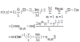
The self-affinity implies that as the surface is repeatedly magnified, more and more surface features appear and the magnified image shows a close resemblance to that of the original surface obtained at a different scale. These properties make the function given by equation (1) suitable for constructing surfaces possessing topographies closely resembling the actual surfaces with the same fractal parameters D and G. the same fractal parameters D and G. Figure 1 shows a sample Weierstrass–Mandelbrot (W–M) surface produced in MATLAB 10.0 using D = 2.3, G = 1.36 × 10⁻¹¹m, l=1e-6, Ls = 1.5×10⁻⁷m, M = 1 and γ = 1.5 (heightscale is in m).
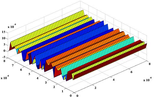
Fig. 1. A sample Weierstrass–Mandelbrot surface.
3. Finite Element Modelling
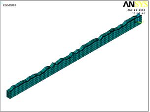
Fig. 2. Geometry of finite element mesh in rough nanobeam.
The finite element analysis is carried out using the static analysis of ANSYS 13.0 which calculates the deflections and stresses produced by the application of the load. MATLAB 10 is used to generate the z (x, y) values from equation (1) as per the supplied x and y values. The points so generated are imported to ANSYS 13.0 as key points. A surface is created by joining the key points. The surface so created is made solid in ANSYS. The rough deformable solid body is modeled using 3D solid element SOLID186, which is defined by twenty nodes having three degrees of freedom at each node. SOLID186 has plasticity, creep, stress stiffening, large deflection, elasticity, nonlinear stabilization, linear perturbation and large strain capabilities. The mesh is kept finer all over the beam in order to take into account variation in the bending stresses. Here the top surface contains the fractal roughness features.
The beam materials studied in this research is single-crystal silicon ].Based on bending experiments, it was found that these beam materials can be assumed to be linearly elastic isotropic materials [11]. Young’s modulus of elasticity (E) and Poisson’s ratio for Si are 169GPa and 0.28 [11]. A sample nano-beam of silicon is chosen for the analysis as silicon is the most widely used MEMS/NEMS material. The cross-section of the fabricated beams used in this study is rectangular and supported at the bottom. So nano-beam with rectangular cross-section is modeled, as shown in Fig. 2. The following dimensions are used width =200nm, thickness =255nm, length =6![]() m. Displacements are constrained in all directions on the bottom surface for 1
m. Displacements are constrained in all directions on the bottom surface for 1 ![]() m from each end. A point load is applied at the center of the beam. It was reported from the experimental results [11] that the load-displacement curve was almost linear and the beam breaks at around 80 µN. Therefore, in the present analysis a nominal load of 70 µN is selected.
m from each end. A point load is applied at the center of the beam. It was reported from the experimental results [11] that the load-displacement curve was almost linear and the beam breaks at around 80 µN. Therefore, in the present analysis a nominal load of 70 µN is selected.
In the analysis, either small or large displacement option can be used. In the small displacement option, linear analysis is performed in which large deformation effects are ignored. The basic assumption is that in beam bending, the slope of deformation of beam axis (dy/dx, where dx and dy are the deformations along the beam axis and orthogonal to the beam axis and the bending plane, respectively) is assumed to be small, no larger than about 0.1. For a beam fixed at both ends, the ratio of maximum displacement (![]() ) and the maximum slope of beam axis
) and the maximum slope of beam axis![]() , is
, is ![]() [18], therefore,
[18], therefore, ![]() /l should be less than 0.03. For a selected load of 70
/l should be less than 0.03. For a selected load of 70 ![]() N, based on FEM analysis of a Si nanobeam,
N, based on FEM analysis of a Si nanobeam, ![]() is 1.42 µm and
is 1.42 µm and ![]() which occurs at l/4 from each ends, is 0.41 [18]. This number is on the higher side for a small displacement analysis. Therefore for the load of interest, large displacement option should be used. However, if small displacement option is used, it should be noted that stresses and displacements are directly proportional to normal load, and values at lower loads can be easily obtained from the small displacement analysis. Accuracy of the FEM results for smooth nano-beam has been verified using analytical beam theory equations for the rectangular beams supported on sides [18,25].
which occurs at l/4 from each ends, is 0.41 [18]. This number is on the higher side for a small displacement analysis. Therefore for the load of interest, large displacement option should be used. However, if small displacement option is used, it should be noted that stresses and displacements are directly proportional to normal load, and values at lower loads can be easily obtained from the small displacement analysis. Accuracy of the FEM results for smooth nano-beam has been verified using analytical beam theory equations for the rectangular beams supported on sides [18,25].
4. Results and Discussion
From the 3D profilometric data, average values of fractal dimension and roughness parameter are chosen for comparative study in the present case as D = 2.4, G = 1.36×10⁻¹¹m. The equivalent Young’s modulus is evaluated as E/(1 − ν2), which is equal to 169GPa and poison’s ratio (v) 0.28.The same material property is used in the finite element solution as well as in the analytical solution [11]. The accuracy of the FEM results is verified using the analytical beam theory equations for the rectangular beam supported at the ends. Figure 3 shows a comparison of the present model with the experimental results.
Fig. 3. A comparison of load-displacement curve of Si nano-beam.
The fractal parameters D andG are chosen in the range typically observed on real rough surfaces. D values are considered in the range between 2.3 and 2.6, and G values are considered in the range between 1.36×10⁻¹³ and 1.36×10⁻¹⁰m.
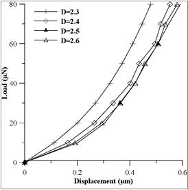
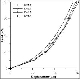
Figure 4(a) shows the plots of load-displacement behavior for a fractal dimension D = 2.3 and varying roughness parameter G. It is seen that at higher G, displacement bears a linear relationship to load while it deviates from linearity at smaller G values and higher loads. Since G is a height scaling parameter, higher G values correspond to rougher (less dense) surface topographies while a decrease in G represents smoother (denser) topography. Thus at a particular load, displacement is larger for lower G values.Fig.4 (b-d) shows the plots of load displacement for fractal dimension D = 2.4, 2.5, 2.6 respectively. And the trend is found to be similar.
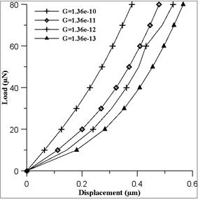
(a)
(b)
(c)
(d)
Fig. 4. Load-displacement curve: effect of varying G, at (a) D=2.3, (b) D=2.4, (c) D=2.5, (d) D=2.6.
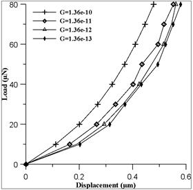
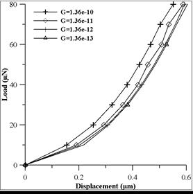
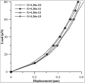
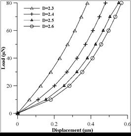
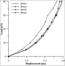
Fig. 5(a) shows the plots of load displacement behavior for fractal roughness parameter ![]() and varying fractal dimension D. It is observed that displacement is proportional to load at small loads and higher D values. But at higher loads and at small D values the rate of change of displacement with load decreases. It means the stiffness of the surface is more for higher D and it increases with load. Fig.5 (b-d) shows the plots of load displacement for other fractal roughness parameters. And the trend is found to be similar.
and varying fractal dimension D. It is observed that displacement is proportional to load at small loads and higher D values. But at higher loads and at small D values the rate of change of displacement with load decreases. It means the stiffness of the surface is more for higher D and it increases with load. Fig.5 (b-d) shows the plots of load displacement for other fractal roughness parameters. And the trend is found to be similar.
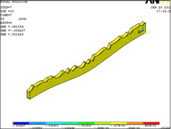
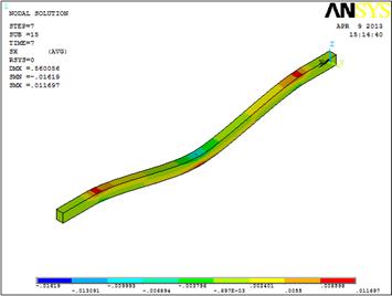
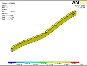
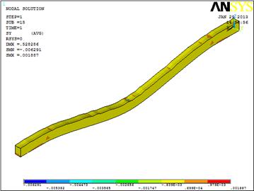
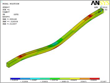
Figures 6 and 7 show topographical stress-field maps where each colour corresponds to a certain stress level range at the surface and at the intersection as shown in the figure. The spherical tip is invisible in order to display the stresses.
(a)
(b)
(c)
(d)
Fig. 5. Load-displacement curve: effect of varying D, at (a) ![]() m (b)
m (b) ![]() m (c)
m (c) ![]() m (d)
m (d) ![]() m.
m.
(a)

(b)

(c)
(d)
Fig. 6. Bending stress contours after loading rectangular Si nanobeam with D=2.4 and (a) ![]() m, (b)
m, (b)![]() m, (c)
m, (c)![]() m, (d)
m, (d)![]() m.
m.
(a)

(b)
(c)
(d)
Fig. 7. Bending stress contours after loading rectangular Si nanobeam with ![]() m. and (a) D=2.3, (b) D=2.4, (c) D=2.5, (d) D=2.6.
m. and (a) D=2.3, (b) D=2.4, (c) D=2.5, (d) D=2.6.
5. Conclusion
FEM simulations are used to predict the stress and deformation in nano-beams. For fixed fractal roughness G, it is seen that increasing fractal dimension increases the displacement at a particular load. Since G is a height scaling parameter, higher G values correspond to rougher (less dense) surface topographies while a decrease in G represents smoother (denser) topography. Thus at a particular load, displacement is larger for lower G values. It is observed that displacement is proportional to load at small loads and higher D values. But at higher loads and at small D values the rate of change of displacement with load decreases. It means the stiffness of the surface is more for higher D and it increases with load. The roughness affects the maximum bending stresses. In a rectangular beam, the maximum tensile stress occurs at the top surface at the ends and the maximum compressive stress occurs at the top surface under the load .The above mentioned observations can be useful to designers to develop the most suitable geometry for nanostructures.
References
- B. Bhushan (Ed.) 2001 Macro and Microtribology of MEMS Materials, Modern Tribology Handbook, CRC Press,Boca Raton, FL, , pp. 1515–48.
- B. Bhushan 1999 Principles and Applications of Tribology, Wiley, New York.
- B. Bhushan (Ed.) 1998 Tribology Issues and Opportunities in MEMS, Kluwer Academic Publisher, Dordrecht, The Netherlands.
- B. Bhushan 1999 Handbook of Micro/Nanotribology,2nd Editon, CRC Press, Boca Raton,FL.
- B. Bhushan 2001Modern Tribology Handbook, Vol.1—Principles of Tribology; Vol. 2—Materials, Coatings,and Industrial Applications, CRC Press, Boca Raton, FL.
- K.E.Peterson 1982 Silicon as a mechanical material, Proc. IEEE 70 420-57.
- S.J ohansson, J.A. Schweitz, L.J. Tiren 1988 Fracture testing of silicon microelements in-situ in a scanning electron microscope, J. Appl. Phys. 63, 4799-4803.
- F.Ericson, J.A.Schweitz 1990 Micromechanical fracture strength of silicon, J. Appl. Phys. 68, 5840-5844.
- C.J. Wilson, A. Ormeggi, M. Narbutovskih 1996 Fracture testing of bulk silicon microcantilever beams, J. Appl. Phys. 79, 2386-93.
- C.J.Wilson, P.A. Beck,1996 Fracture testing of bulk silicon microcantilever beams subjected to a side load, J. Microelectromech. Syst. 5, 142-150.
- S. Sundararajan, B. Bhushan 2002 Development of AFM-based techniques to measure mechanical properties of nanoscale structures,Sensors and Actuators A 101,338-51.
- T. Hsu, N. Sun, Residual stresses/strains analysis of MEMS, in: M. Laudon, B. Romanowicz (Eds.), Proceedings of the International Conference on Modeling and Simulation of Microsystems, Semiconductors, Sensors and Actuators, Computational Publications, Cambridge, MA,1998, pp. 82–87.
- J.H. Fabian, L. Scandella, H. Fuhrmann, R. Berger, T. Mezzacasa, Ch. Musil, J. Gobrecht, E. Meyer, Ultramicroscopy 82 (2000) 69.
- A. Kolpekwar, C. Kellen, R.D. Blanton, Fault model generation for MEMS, in: M. Laudon, B. Romanowicz (Eds.), Proceedings of the International Conference on Modelingand Simulation of Microsystems, Semiconductors, Sensors and Actuators, Computational Publications, Cambridge, MA, 1998, pp. 111–116.
- H.A. Rueda, M.E. Law, Modeling of strain in boron-doped silicon cantilevers, in: M. Laudon, B. Romanowicz (Eds.), Proceedings of the International Conference on Modeling and Simulation of Microsystems, Semiconductors, Sensors and Actuators, Computational PublicationsCambridge MA, 1998, pp. 94–99.
- M. Heinzelmann, M. Petzold 1994 FEM analysis of microbeam bending experiments using ultra micro indentations,Comput. Mater. Sci. 3, 169-76.
- B. Bhushan and G.B. Agrawal 2002 Stress analysis of nanostructures using a finite element method, Nanotechnology 13, 515-23.
- R.J. Roark, Roark’s Formulas for Stress and Strain, 6th Edition, McGraw-Hill, New York, 1989.
- P. Sahoo and N. Ghosh 2007 Finite element contact analysis of fractal surfaces, J.Appl.Phys.40, 4245-52.
- W Yan and K Komvopoulos 1998 Contact analysis of elastic-plastic fractal surfaces, J.Appl.Phys.84, 3617-24.
- M Ausloos and D H Berman D H 1985 A multivariate Weierstrass-Mandelbrot function, Proc. R. Soc. Lond. A 400, 331-50.
- M V Berry and Z V Lewis 1980 On the Weierstrass-Mandelbrot fractal function, Proc. R. Soc. Lond. A 370, 459-84.
- D Blackmore and J G Zhou 1998 Fractal analysis of height distributions of anisotropic rough surfaces, Fractals 6, 43-58.
- S Bhattacharyya and S Sahoo 2014 Stress analysis of trapezoidal nanobeam with roughness, International Journal of Materials, Manufacturing and Design, 2(1-2), 29-44.
- S Bhattacharyya, S Sahoo and P Sahoo 2014 Finite element based analysis of nanobeam with fractal roughness, International Journal of Applied Engineering Research, 9(26), 8803-8806.


