
Journal of Nanoscience and Nanoengineering, Vol. 1, No. 2, August 2015 Publish Date: Aug. 6, 2015 Pages: 56-65
Modified Parameter of Tight Binding Model to Calculate First and Second Optical Transition Energies of Semiconducting SWCNTs
G. R. Ahmed Jamal1, *, S. M. Mominuzzaman2
1Department of Electrical and Electronic Engineering, University of Asia Pacific, Dhaka, Bangladesh
2Department of Electrical and Electronic Engineering, Bangaldesh University of Engineering and Technology, Dhaka, Bangladesh
Abstract
In this work, an empirical model of nearest neighbor hopping parameter (γ0) in tight binding (TB) model of single wall carbon nanotubes is proposed in order to calculate first and second optical transition energies of semiconducting SWCNTs. A highly systematic and nearly linear pattern is observed when the γ0, as calculated from experimental optical transition energies of semiconducting SWCNTs, were scaled by a chirality combination term (2n-m) and plotted against tube diameters. Based on this observation, two empirical expressions of γ0 are formulated for mod 1 and mod 2 type semiconducting SWCNTs. In this model of γ0, observations from various optical spectroscopic experiments are incorporated. First and second optical transition energies (E11 and E22) for all semiconducting SWCNTs within diameter range of 0.4 to 3 nm are calculated using this empirical γ0. Calculated values showed excellent agreement with experimental values for all type of chiralities over the full diameter range and precisely reflected the chirality effect on transition energies. The proposed empirical γ0 highly improved the calculation from simplest tight binding model and enables it to give almost accurate qualitative and quantitative prediction of first two transition energies of semiconducting SWCNTs.
Keywords
Nanotube, SWCNT, Optical Transition Energy, Chiral Index, Hopping Parameter, Empirical
Received: July 9, 2015
Accepted: July 26, 2015
Published online: August 6, 2015
@ 2015 The Authors. Published by American Institute of Science. This Open Access article is under the CC BY-NC license. http://creativecommons.org/licenses/by-nc/4.0/
Contents
1. Introduction
Since the discovery of Carbon Nanotubes (CNT) by Sumio Iijima [1,2] in 1991, they become one of the most intensively studied materials and are gaining more and more attention to researchers in every year. For their unique one-dimensional nanostructure and extraordinary electronic, optical, mechanical and chemical properties, CNTs are considered as an ideal building block for next-generation molecular electronic and optoelectronic devices and circuits [3,4].
Electronic and optical properties of single-wall carbon nanotubes (SWCNT) are directly associated with their geometrical structures [5,6] which are uniquely specified by a pair of chiral index (n, m). A SWCNT (n, m) will be metallic if its n-m = 3k (k is integer), i.e. mod(n-m, 3) = 0 and it will be semiconducting if its n-m ≠ 3k, i.e. mod(n-m, 3) = 1 or 2, which is always found true except for tubes with too small diameters [7]. This relation gives two types of semiconducting SWCNTs, mod 1 type and mod 2 types. Also, this relation indicates that theoretically two third of the total SWCNTs are semiconducting and one third are metallic.
The one-dimensionality of the nanotubes gives rise to 1D subbands instead of one wide electronic energy band in nanotube density of states. Each SWCNT (n, m) has a unique set of interband energies Eii denoting the energy differences between the i-th conduction and valence bands and optical transitions can only occur between these mirror subbands [5,6,8,10]. These singularities are unique feature of nanotubes and also primarily responsible for many distinguished electronic and optical properties of SWCNTs.
The tight-binding (TB) model of π-bands of graphene using the zone-folding approximation has been widely used for modeling electronic band structure of single-wall carbon nanotube (SWCNT) due to its simplicity, low computational cost, and good qualitative agreement with experimental results [11-13]. TB model with the nearest-neighbor approximation provides following simple expression to calculate optical transitions of a semiconducting nanotubes [5,6,14]:
![]() (1)
(1)
Where, ![]() is the nearest-neighbor hopping parameter,
is the nearest-neighbor hopping parameter, ![]() Å is carbon-carbon bond length,
Å is carbon-carbon bond length, ![]() is nanotube diameter in nm, given by
is nanotube diameter in nm, given by ![]() and j is an integer. Eii corresponds to the first, second, third, fourth…… interband transitions (E11, E22, E33, E44….) of semiconducting SWCNTs when j = 1, 2, 4, 5… respectively. This inverse proportional relation of optical transitions with diameter is also observed in well-known Kataura plot [15]. Here, the first optical transition (E11) is the bandgap of semiconducting SWCNTs and the information on second optical transition (E22) facilitates various optical spectroscopic experiments, as it falls within visible energy range. Also, for photo absorption, first two optical transitions are mainly considered. Hence, E11 and E22 of semiconducting SWCNTs are more significant than other transitions and are of more interest.
and j is an integer. Eii corresponds to the first, second, third, fourth…… interband transitions (E11, E22, E33, E44….) of semiconducting SWCNTs when j = 1, 2, 4, 5… respectively. This inverse proportional relation of optical transitions with diameter is also observed in well-known Kataura plot [15]. Here, the first optical transition (E11) is the bandgap of semiconducting SWCNTs and the information on second optical transition (E22) facilitates various optical spectroscopic experiments, as it falls within visible energy range. Also, for photo absorption, first two optical transitions are mainly considered. Hence, E11 and E22 of semiconducting SWCNTs are more significant than other transitions and are of more interest.
The qualitative agreement of Eqn (1) with experimental results is good [11], but quantitatively it underestimates and overestimates E11 and E22 of semiconducting SWCNTs around 25% even with the best choice of ![]() as a fitting constant parameter [16]. Equation (1) also fails to reflect relative difference between mod 1 and mod 2 type semiconducting SWCNTs for odd (E11S, E33S,….) and even (E22S, E44S,….) transitions with comparable diameter [17], and gives incorrect ratio of first two optical trasnsitions [18], as observed from various optical spectroscopic experiments.
as a fitting constant parameter [16]. Equation (1) also fails to reflect relative difference between mod 1 and mod 2 type semiconducting SWCNTs for odd (E11S, E33S,….) and even (E22S, E44S,….) transitions with comparable diameter [17], and gives incorrect ratio of first two optical trasnsitions [18], as observed from various optical spectroscopic experiments.
These disagreements of Eqn (1) are attributed to many factors. One major factor is nanotube ‘curvature effect’ induced band structure deviation from simple π-orbital graphene picture [19-22]. Other factors are ‘chirality effect’ [23], ‘trigonal warping effect’ [17,19,24] and many body effect (electron-electron interaction) comprising self-energy and exitonic effect [25-30].
Considering these limitations of TB model, several authors [11,13,16,18,20,22,24,30,43] tried to improve TB model calculation of electronic band structure of SWCNTs so as to fit it with various experimental observations. Some of them just extended simple π-band model to get better calculation. Some proposed modified or alternative model within or beyond the TB model approach and showed improved calculation using that. Some of them tried to improve TB model Eqn (1) by including extra terms with it, deduced theoretically or empirically. Some took pure empirical approach and proposed model independent empirical equations, without caring Eqn (1).
One common factor in all the above mentioned theoretical and empirical approaches is, they tried to include chirality effect always in the form of a specific term {cos (3θ)} [16,18,22,34,43] and did not consider any other combination of chiral indices. Another common point is, they all considered the nearest neighbor hopping parameter, γ0, merely as a fitting constant. Though Ding et al [23] proposed to modify the hopping parameter γ0, they mainly considered curvature effect on γ0 while ignored rest other effects [26].
The overall issue can be alternatively addressed if curvature, chirality and other effects are included in γ0, instead of directly adding an extra term with Eqn (1) so as to keep the basic form of TB model Eqn (1) intact. In fact, ![]() was considered as a constant only in earlier works [5-10,13,15,20,24] where they took it merely as a fitting parameter but they never get unified on any fixed value. Values from 2.4 to 3.2 or above are reported in different literatures [24,32], of which 2.7 and 2.9 have been preferred and used in most of the cases. Later, it was realized that deviation of Eqn (1) from experimental observations is partly because of taking
was considered as a constant only in earlier works [5-10,13,15,20,24] where they took it merely as a fitting parameter but they never get unified on any fixed value. Values from 2.4 to 3.2 or above are reported in different literatures [24,32], of which 2.7 and 2.9 have been preferred and used in most of the cases. Later, it was realized that deviation of Eqn (1) from experimental observations is partly because of taking ![]() as a constant [23,32,44,45]. Idea of a constant
as a constant [23,32,44,45]. Idea of a constant ![]() is no longer appreciated now and many later authors [23,24,32,44] proposed its dependency on nanotube structure. So an approach of taking
is no longer appreciated now and many later authors [23,24,32,44] proposed its dependency on nanotube structure. So an approach of taking ![]() as a parameter whose value will depend on nanotube structure so as to reflect various observed effects is quite justified and can be proven more effective than earlier attempts. Also, as classifying semiconducting SWCNT in mod 1 and mod 2 type originates from chirality (n, m), not from chiral angle, so chirality effect on optical transitions can be reflected through alternative combination of chiral index (n, m) other than the chiral angle.Calculation of first and second optical transition energies (E11S and E22S) of semiconducting SWCNTs from simple TB model, as represented by Eqn. (1), can be improved significantly if its most important parameter, namely the hopping parameter (γo) is modeled properly.
as a parameter whose value will depend on nanotube structure so as to reflect various observed effects is quite justified and can be proven more effective than earlier attempts. Also, as classifying semiconducting SWCNT in mod 1 and mod 2 type originates from chirality (n, m), not from chiral angle, so chirality effect on optical transitions can be reflected through alternative combination of chiral index (n, m) other than the chiral angle.Calculation of first and second optical transition energies (E11S and E22S) of semiconducting SWCNTs from simple TB model, as represented by Eqn. (1), can be improved significantly if its most important parameter, namely the hopping parameter (γo) is modeled properly.
The main objective of this work is to present an effective model of the tight binding hopping parameter (γo), so as to give nearly accurate prediction of first two optical transitions in semiconducting SWCNTs. To achieve this objective, the tight binding model parameter will be designed in such a way so that it can accommodate various experimental observations in a much better way than the simple TB model.
2. Method
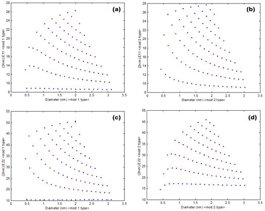
Figure 1. (a) (2n-m).E11 vs dt plot for mod 1 type SWCNTs, (b) (2n-m).E11 vs dt plot for mod 2 type SWCNTs, (c) (2n-m).E22 vs dt plot for mod 1 type SWCNTs, (d) (2n-m).E22 vs dt plot for mod 2 type SWCNTs.
In this work, all the SWCNTs in between diameter ~0.4 nm to ~3 nm are considered. Then, all semiconducting SWCNTs within this diameter range are selected by applying the n-m=3k or ≠3k condition, where k is a positive integer. In this way, total 212 semiconducting SWCNTs were found, comprising both zigzag and chiral tubes. Metallic tubes are excluded as they are not the concern in this work. Chiral index of these semiconducting SWCNTs, within this diameter range, starts from (4, 2) tube with diameter 0.42 nm and extends up to (23, 22) tube with diameter 3.094 nm. After sorting them according to their mod value, we found 110 mod 1 type and 102 mod 2 type semiconducting SWCNTs.
Values of first and second optical transition energies (ev) corresponding to all these semiconducting SWCNTs are recorded from multiple reports of different optical spectroscopic experiments [10,14,16,18,32,34,37,46,65]. As only semiconducting tubes are being considered here, so, from now on first and second optical transition energies will be denoted simply as E11 and E22. Recorded data showed that E11 for mod 2 types are higher than that of mod 1 type whereas E22 for mod 2 types are lower than that of mod 1 type with comparable diameters. In order to reflect this phenomenon, it will be suitable to propose and formulate two separate γ0 for mod 1 and mod 2 type semiconducting SWCNTs. It may help to reflect unique trend of both of these groups more precisely.
In order to devise separate γ0 for each mod type, transition energies of mod 1 and mod 2 semiconducting SWCNTs were studied separately to reveal their specific relation with diameter, chiral index and mod value. Few things were noticed from close observation of this wide range of data. It was observed that even within a particular mod type, though the first and second optical transition energies decrease in general with increasing diameters, as predicted by basic TB model equation (1), but this decreasing pattern is not smooth. It does not follow simple 1/dt relation, rather it follows a continuous nonlinear ups and downs for each tube, which may originates from their individual chirality. These ups and downs are more prominent in lower diameter tubes and negligible only for tubes with diameters above 2.5 nm, i.e. it is noticeable up to 80% of the total diameter range. In earlier attempts by others, such variation was tried to be reflected by inclusion of the chiral angle term cos (3θ). An alternative idea can be to reflect this variation in terms of more direct combination of chiral index (n, m) term instead of chiral angle. In fact, classifying semiconducting SWCNTs in mod 1 and mod 2 types originates directly from their chiral index, not chiral angle. So, there can be a direct relation of these ups and downs with a suitable chiral index combination. In order to reveal possible chiral index dependence of optical transition energies, both E11 and E22 are scaled by some random combination of their chiral index and plotted the scaled transition energies against their diameters. The changes in those sharp ups and downs were closely investigated after this scaling and interestingly, it was found that their rise and down trend exhibits highly systematic patterns when they are scaled with a specific chiral index combination (2n-m). This scaling effect can be observed from Fig. 1 (a) to (d) where, E11 vs dt and E22 vs dt plots are shown after scaling by (2n-m). Though mod 1 type and mod 2 types were studied separately for first and second optical transition energies, this systematic pattern with (2n-m) term is commonly observed for both types of semiconducting SWCNTs in both optical transition energies, as shown in these Figures.
This important finding enables to reflect chirality effect in terms of this (2n-m) term for better tracing of experimental data. Now, as the objective here is to devise a model for tight binding hopping parameter (γo), that will be used for calculating optical transitions, this (2n-m) scaling effect on transition energies need to be included in that model of γo. If this (2n-m) term can be properly incorporated in the model of γo, then the calculated optical transitions from the model may precisely reflect the chirality effect and corresponding ups and downs for any chirality.
To build a proper model of γo, the variation trend of values of γo for different chiralities and diameters need to be observed. For this, the values of γo from Eqn (1) is calculated, using dt and experimental values of E11 for each semiconducting SWCNTs, as
![]()
γo found in this way may be termed as ‘experimental γo. These calculated γo values were divided into two sets: one set originates from mod 1 type and another set originate from mod 2 type. These two sets of γo can be plotted against corresponding dt to observe their variation with respect to dt and various chiralities.
Now, as mentioned before, appropriate way has to be found out to include the term (2n-m) in the model of γo so as to reflect the chirality effect on transition energies. For this, γo of both mod types can be scaled by this term and can be plotted again against dt so as to see the change in previous γo vs dt plots and to find whether they follow any systematic pattern like optical transitions. These γovs dt plots for both mod types, before and after scaling by (2n-m), are shown in Fig. 2 (a) and (b). From these Figures, it was clearly noticed that, when γo of both mod types are scaled by (2n-m) and then plotted against dt, they exhibit highly systematic patterns. The systemic patterns followed by these plots of scaled γo are more smooth and regular than corresponding plots of scaled transition energies. Moreover, the patterns of the dotted lines in both plots are now nearly linear.
All these observations suggest reflecting chirality effect in terms of this (2n-m) term for better tracing of experimental transition energies. These also show how to include this term in devising the model of γo, so as to predict optical transition energies in a better way from the modeled γo.
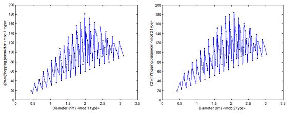
Figure 2. (a) (2n-m)γo vs dt plot for mod 1 type semiconducting SWCNTs and (b) (2n-m)γo vs dt plot for mod 2 type semiconducting SWCNTs.
Now, if Fig. 2 (a) and (b) are observed closely, nearly linear pattern of (2n-m)γo vs dt plots is noticed for both mod types (scaled values of γo are indicated by black dots which reveals their linear pattern). This observation tells that (2n-m)γo for both mod 1 and mod 2 types approximately can be considered linearly proportional to dt , i.e. (2n-m)γo = p dt + q (where p and q are arbitrary constant)
Hence, a term in the form of (p dt + q)/(2n-m) can be included in the model of γo in order to reflect chirality effect. Also, as the the directions of variation of values of γo are opposite for mod 1 and mod 2 types, so, p and q should take opposite signs for mod 1 and mod 2 type semiconducting SWCNTs.
Hence, one component of the proposed model is devised, i.e. a term with above form to be included in our target model of γo in order to reflect ‘chirality effect’. It is important to note that ‘chirality effect’ mainly accounts precise ups and downs of transition energies for both mod types that arise from individual tube chirality. But, ‘chirality effect’ alone cannot account all the quantitative deviations of Eqn (1) from experimental results, as there are other two important effects namely ‘curvature effect’ and ‘trigonal warping effect’ also. Hence, these effects need to be addressed as well and corresponding components have to be devised to be included in the proposed model to reflect these effects. Then the model will be completed.
‘Curvature effect’ originates from nanotube curvature. This effect is very dominant for lower diameter tubes (dt < 2 nm) and one of the main causes of quantitative deviation of Eqn (1) from experimental results. Fortunately, expressing ‘curvature effect’ is comparatively easy and less ambiguous. As diameter dt is directly responsible for tube curvature, so suitable inclusion of dt term can reflect this effect. ‘Trigonal warping effect’ is another significant effect that also depends on dt. Hence, intelligent placing of two dt terms in proposed empirical equation can account both the effects. Now, in the already devised expression of ‘chirality effect’, the effect of chirality is specificly represented by the denominator term (2n-m) as it is the scaling factor to generate those systematic patterns in corresponding plots, whereas the dt term in nominator partially account ‘curvature effect’ and ‘trigonal warping effect’ up to some degree. As a dt term is already present there, so, only one more dt term is needed in the proposed model of γo to balance rest two effects. Some of the observations on the behavior of mod 1 and mod 2 type’s optical transitions in kataura plot may give some clue on how to add this another dt term in the model of γo. It was observed earlier that relative higher or lower values for mod 1 and mod 2 types alternate for odd and even transitions, i.e. E11mod1 <E11mod2 but E22mod1 > E22mod2. So, mod 1’s E22 follow the trend of mod 2’s E11, and mod 2’s E22 follow the trend of mod 1’s E11. The opposite trend of mod 1 and mod 2 branches in kataura plot suggests that the proposed another dt term should appear in the model of γo in two opposite forms for the two mod types in order to reflect this obsevation: one as proportional to 1/dt and another as proportional to dt. So, now necessary components are gathered to be added in the model of γo in order to reflect ‘chirality effect’, ‘curvature effect’ and ‘trigonal warping effect’.
Another effect namely many body effect or self-energy and exitonic effect is not included or adjusted here as it was not found necessery. A recent study of Sato et al [66] showed that, for E11 and E22 transitions, the chirality dependence of the exciton binding energy for each (n,m) SWCNT is almost cancelled by that of the self energy, both effects being of the same order of magnitude. As per their analysis, the origin of the family pattern for E11 and E22 can be understood by the chirality dependence of the single particle energies, by safely ignoring many body effect. Also, any pre-defined or specific term cannot be included to account these effects as the nature and amount of these effects are still being discussed in literatures and also much disputed. So, this effect can be ignored in the proposed model.
After setting all necessary tools to devise the proposed empirical expression for γo, as a last step, all the previous theoretical and empirical efforts [11,13,16,18,20,22,24,30,43] of predicting transition energies were re-examined to avoid their shortcomings. For chirality effect nothing from those equations need not to be taken as we devised our own term (2n-m) to reflect it. Rest other terms will be suitably arranged around this (2n-m) term. For including curvature effect and trigonal warping effect some insights from earlier equations is taken but those are reflected here in a new way, based on our own observations. Two dt terms are included in the proposed empirical expression of γo to reflect ‘curvature effect’ and ‘trigonal warping effect’. Rest other minor and undefined effects will be adjusted within numerical fitting parameters. One main intention is to make the proposed empirical expression simpler than earlier expressions, while giving much higher accuracy than those equations. Another intention is to keep the basic form of simple TB model derived equation intact by modifying its hopping parameter γo only.
3. Result
Finally, combining all these in depth observations over this wide range of data with the insights found from earlier equations, a smart model or empirical expression of γ0 is proposed, by summing up our earlier devised components to reflect ‘curvature effect’, ‘chirality effect’ and ‘trigonal warping effect’. A set of empirical equations for nearest-neighbor hopping parameter γ0 are formulated, separately for mod 1 and mod 2 types, so as to give nearly accurate prediction of first and second optical transition energies of semiconducting SWCNTs using this γ0. Devised set of empirical equations are presented below one by one:
Eqn (1) gives first optical transition energy of semiconducting SWCNTs for i=1, j=1,
![]() (2)
(2)
But, to express second optical transition energy (E22), j = 2 cannot be used, since experimental observation showed that ratio of E22 to E11 is not 2, as mentioned earlier. So, in order to facilitate the calculation, their observed ratio is empirically expressed for both mod 1 and mod 2 types as r1 and r2, where,
![]()
and, ![]()
Hence, instead of putting j = 2, here j = r1 and r2 will be used to calculate E22 for mod 1 and mod 2 types, respectively. Accordingly, Expression of E22 from Eqn (1) becomes,
For mod 1:
![]()
![]() (3)
(3)
And for mod 2:
![]()
![]() (4)
(4)
Finally, the core equations will be presented, i.e. the formulated empirical expression for ![]() to calculate E11 and E22 precisely,
to calculate E11 and E22 precisely,
![]() to calculate E11 (for mod 1 type) and E22 (for mod 2 type):
to calculate E11 (for mod 1 type) and E22 (for mod 2 type):
![]() (5)
(5)
![]() to calculate E11 (for mod 2 type) and E22 (for mod 1 type):
to calculate E11 (for mod 2 type) and E22 (for mod 1 type):
![]() (6)
(6)
It can be noted that same ![]() is used in calculating both E11 and E22 for alternative mod type. This comes from the earlier mentioned observation that relative higher or lower values for mod 1 and mod 2 types alternate for odd and even transitions, i.e. E11mod1 < E11mod2 but E22mod1 > E22mod2. So, mod 1’s E11 follows same trend like mod 2’s E22 and hence same
is used in calculating both E11 and E22 for alternative mod type. This comes from the earlier mentioned observation that relative higher or lower values for mod 1 and mod 2 types alternate for odd and even transitions, i.e. E11mod1 < E11mod2 but E22mod1 > E22mod2. So, mod 1’s E11 follows same trend like mod 2’s E22 and hence same ![]() can be used for both, as emperical r1 and r2 are already there to scale E22.
can be used for both, as emperical r1 and r2 are already there to scale E22.
Equation (5) and (6) generate values of ![]() for mod 1 and mod 2 types SWCNTs, depending on their
for mod 1 and mod 2 types SWCNTs, depending on their ![]() and (2n-m) terms to reflect curvature effect, trigonal warping effect and chirality effect. Rest other effects, in generallly, may be thought to be adjusted within associated numerical fitting parameters though we do not suggest specific meaning of these numerical terms within nanotube electronic structure.
and (2n-m) terms to reflect curvature effect, trigonal warping effect and chirality effect. Rest other effects, in generallly, may be thought to be adjusted within associated numerical fitting parameters though we do not suggest specific meaning of these numerical terms within nanotube electronic structure.
Generated ![]() from Empirical Eqn (5) and (6) was found to vary from 2.22 to 3.86 for mod 1 and from 3.22 to 3.86 for mod 2 over the full diameter range. To check whether this variation is fair, real
from Empirical Eqn (5) and (6) was found to vary from 2.22 to 3.86 for mod 1 and from 3.22 to 3.86 for mod 2 over the full diameter range. To check whether this variation is fair, real ![]() may be calculated from Eqn (2) using experimental values of E11. Amazingly, it gives exactly the same range of variation.
may be calculated from Eqn (2) using experimental values of E11. Amazingly, it gives exactly the same range of variation.
Table I. Comparison of experimental and empirical results for E11 and corresponding average error and % average error for two mod types.
| Diameter () | MOD 1 Type | MOD 2 Type | ||
| Avg | Avg | Avg | Avg | |
| 0.4 nm ≤ dt ≤ 3 nm | 0.0036 | 0.43% | 0.0033 | 0.32% |
| 1 nm ≤ dt ≤ 3 nm | 0.0023 | 0.36% | 0.0015 | 0.20% |
| 1.5 nm ≤ dt ≤ 3 nm | 0.0015 | 0.29% | 0.0006 | 0.11% |
Table II. Comparison of experimental and empirical results for E22 and corresponding average error and % average error for two mod types.
| Diameter () | MOD 1 Type | MOD 2 Type | ||
| Avg | Avg | Avg | Avg | |
| 0.4 nm ≤ dt ≤ 3 nm | 0.0115 | 0.66% | 0.0083 | 0.57% |
| 1 nm ≤ dt ≤ 3 nm | 0.0052 | 0.46% | 0.0037 | 0.35% |
| 1.5 nm ≤ dt ≤ 3 nm | 0.0037 | 0.39% | 0.0031 | 0.33% |
First and second optical transition energies (E11 and E22) of all 212 semiconducting SWCNTs were calculated from Eqn (2), (3) and (4) using ![]() from Eqn (5) and (6) for mod 1 and mod 2 types. The calculated E11 and E22 showed excellent match from lowest diameter (0.4 nm) to highest diameter (3 nm). The plots of E11 vs
from Eqn (5) and (6) for mod 1 and mod 2 types. The calculated E11 and E22 showed excellent match from lowest diameter (0.4 nm) to highest diameter (3 nm). The plots of E11 vs ![]() and E22vs
and E22vs ![]() for both mod 1 and mod 2 types are shown in Figure 3. The agreement between experimental and empirical graphs over the full diameter range is so good as if they are replica of each other. Enlarged portions of the plots in (b) show this precise tracing more closely.
for both mod 1 and mod 2 types are shown in Figure 3. The agreement between experimental and empirical graphs over the full diameter range is so good as if they are replica of each other. Enlarged portions of the plots in (b) show this precise tracing more closely.
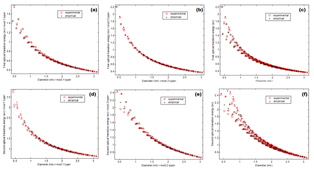
Figure 3. Comparing experimental and empirical values of (a) E11 of mod 1 type (b) E11 of mod 2 type (c) E11 of both mod types with our empirically calculated E11 (d) E22 of mod 1 type with our empiricallay calculated E22 (e) E22 of mod 2 types (f) E22 of both mod types.
The overall comparison between the empirical data and experimental data is summarized in Table I and table II for E11 and E22, respectively. Table I shows that average absolute deviations (![]() ) and % average absolute deviations (
) and % average absolute deviations (![]() ) of empirical data for E11 are very low and within tolerable margin. Average error for E11 over full diameter range is 0.0036 eV (0.43%) and 0.0033 eV (0.32 %) for mod 1 and mod 2, respctively. Same things can be noticed from Table II where average error for E22 over full diameter range is 0.0113 eV ( 0.65%) and 0.0081 eV (0.56 %) for mod 1 and mod 2, respectively. In both cases,
) of empirical data for E11 are very low and within tolerable margin. Average error for E11 over full diameter range is 0.0036 eV (0.43%) and 0.0033 eV (0.32 %) for mod 1 and mod 2, respctively. Same things can be noticed from Table II where average error for E22 over full diameter range is 0.0113 eV ( 0.65%) and 0.0081 eV (0.56 %) for mod 1 and mod 2, respectively. In both cases, ![]() and
and ![]() reduces more for increasing diameters as shown in Table I and II.
reduces more for increasing diameters as shown in Table I and II.
Hence, the proposed empirical expression of ![]() enables Eqn (1) to give almost accurate prediction of first and second optical transition energies of mod 1 and mod 2 types semiconducting SWCNTs with less than 1% average absolute error over the full the diameter range and with less than 0.5% average absolute error for diameters above 1 nm. It removes earlier shortcomings of the basic equation derived from simple TB model and can calculate optical transitions for both zigzag and chiral tubes with same accuracy. Most importantly, it gives almost same level of accuracy for lower and higher diameter tubes and hence strengthens nearest neighbor tight binding model which is commonly accused for being highly inaccurate in lower diameter tubes.
enables Eqn (1) to give almost accurate prediction of first and second optical transition energies of mod 1 and mod 2 types semiconducting SWCNTs with less than 1% average absolute error over the full the diameter range and with less than 0.5% average absolute error for diameters above 1 nm. It removes earlier shortcomings of the basic equation derived from simple TB model and can calculate optical transitions for both zigzag and chiral tubes with same accuracy. Most importantly, it gives almost same level of accuracy for lower and higher diameter tubes and hence strengthens nearest neighbor tight binding model which is commonly accused for being highly inaccurate in lower diameter tubes.
4. Conclusions
In this work, at first we have highlighted the limitations of basic tight binding model to calculate first and second optical transitions in SWCNTs. To solve this problem, we proposed an empirical model of nearest neighbor hopping parameter (γ0) in tight binding (TB) model of single wall carbon nanotubes in order to calculate first and second optical transition energies of semiconducting SWCNTs. We observed a highly systematic pattern when the γ0, as calculated from experimental optical transition energies of semiconducting SWCNTs, were scaled by a chirality combination term (2n-m) and plotted against tube diameters. Based on this observation, two empirical expressions of γ0 were formulated for mod 1 and mod 2 type semiconducting SWCNTs. In this model of γ0, observations from various optical spectroscopic experiments are incorporated. First and second optical transition energies (E11 and E22) for all semiconducting SWCNTs within diameter range of 0.4 to 3 nm are calculated using this empirical γ0. Calculated values showed excellent agreement with experimental values for all type of chiralities over the full diameter range. The average absolute error between predicted and experimental data was lesser than 0.5% both transitions. The proposed empirical γ0 highly improved the calculation from simplest tight binding model and enables it to give almost accurate qualitative and quantitative prediction of first two transition energies of semiconducting SWCNTs.
References
- S. Iijima, "Helical microtubules of graphitic carbon", Nature 354, pp.56 – 58, 1991.
- S. Iijima and T. Ichihashi, "Single-shell carbon nanotubes of 1-nm diameter", Nature 363, pp.603 – 605, 1993.
- A. P. Graham, G.S. Duesberg, W. Hoenlein, F. Kreupl, M. Liebau, R. martin, B. Rajasekharan, W. Pamler, R. Seidel, W. Steinhoegl, E. Unger, "How Do Carbon Nanotubes Fit into the Semiconductor Roadmap?", Appl. Phys. A, 80, pp.1141–1151, 2005.
- Kahng, B. Andre, "Scaling: More than Moore's law", Design and Test of Computers, IEEE, Vol. 27, Issue 3, pp. 86 – 87, 2010.V. N. Popov, "Carbon nanotubes: properties and application", Materials Science and Engineering R, 43, pp. 61–102, 2004.
- V. N. Popov, "Carbon nanotubes: properties and application", Materials Science and Engineering R, 43, pp. 61–102, 2004.
- T. W. Odom, J. L. Huang, P. Kim, and C. M. Lieber, "Structure and Electronic Properties of Carbon Nanotubes",J. Phys. Chem. B,104,pp.2794-2809, 2000.
- N. Hamada, S. Sawada, and A. Oshiyama, "New one-dimensional conductors: graphitic microtubules," Phys. Rev. Lett., Vol.68,No.10,pp.1579-1581, 1992.
- J. W. Mintmire and C. T. White, "Universal density of states for carbon nanotubes", Phys. Rev. Lett., Vol. 81, No.12, 1998.
- S. Reich and C. Thomsen, "Chirality dependence of the density-of-states singularities in carbon nanotubes", Phys. Rev. B, Vol 62, No. 7, 2000.
- M.S. Dresselhausa, G. Dresselhausc, A. Jorio, A.G. Souza Filho, R. Saito, "Raman spectroscopy on isolated single wall carbon nanotubes", Carbon, 40, pp.2043–2061, 2002.
- J. D. Correa, A. J. R. da Silva, and M. Pacheco, "Tight-binding model for carbon nanotubes from ab initio calculations," J. Phys.: Condens. Matter, Vol.22,No.7, 275503, 2010.
- R. Kundu, "Tight binding parameters for graphene", Modern Physics Letters B, Vol. 25, No. 3, pp.163-173, 2011.
- S. Reich, J. Maultzsch, and C. Thomsen, "Tight-binding description of graphene," Phys. Rev. B, Vol.66,No.3,pp.035412, 2002.
- Y. Lian, Y. Maeda, T. Wakahara, T. Akasaka, S. Kazaoui, N. Minami, N. Choi and H. Tokumoto, "Assignment of the Fine Structure in the Optical Absorption Spectra of Soluble Single-Walled Carbon Nanotubes", J. Phys. Chem. B, 107, 12082-12087, 2003.
- H. Kataura, Y. Kumazawa, Y. Maniwa, I. Umezu, S. Suzuki, Y. Ohtsuka, and Y.Achiba, "Optical properties of single-wall carbon nanotubes," Synthetic Met., Vol.103,pp.2555, 1999.
- R. B. Weisman and S. M. Bachilo, "Dependence of optical transition energies on structure for single-walled carbon nanotubes in aqueous suspension: an empirical kataura plot," Nano Lett., Vol.3,No.9,pp.1235-1238, 2003.
- M. Y Sfeir., T.Beetz, F Wang, L.Huang, X. M. H Huang., M.Huang, J. Hone, S. O’Brien, J. A Misewich, T. F.Heinz, L.Wu, Y.Zhu, L. E. Brus, "Optical Spectroscopy of Individual Single-Walled Carbon Nanotubes of Defined Chiral Structure", Science, Vol. 312, April 2006.
- Bachilo S. M., Strano M. S., Kittrell C., Hauge R. H., Smalley R. E., Weisman R. B., "Structure-Assigned Optical Spectra of Single-Walled Carbon Nanotubes", Science, Vol 298 No. 5602, pp.2361, 2002.
- V. Zólyomi and J. Kürti, "First-principles calculations for the electronic band structures of small diameter single-wall carbon nanotubes", Phys. Rev. B 70, 085403, 2004.
- V. N. Popov,"Curvature effects on the structural, electronic and optical properties of isolated single-walled carbon nanotubes within a symmetry-adapted non-orthogonal tight-binding model",New Journal of Physics,Vol. 6,2004.
- H. Zeng, H. F. Hu, J. W. Wei, Z. Y. Wang, L. Wang, and P. Peng, "Curvature effects on electronic properties of small radius nanotube," Appl. Phys. Lett., Vol.91,No.3,pp.033102, 2007.
- O. Gulseren, T. Yildirim and S. Ciraci,"A systematic ab-initio study of curvature effects in carbon nanotubes", Phys. Rev. B 65, 153405, 2002.
- J W Ding, X H Yan, J X Cao, "Analytical relation of band gaps to both chirality and diameter of single-wall carbon nanotubes", Phys. Rev. B , Vol. 66, Issue 7, Pages: 2-5, 2002.
- R. Saito, G. Dresselhaus, and M. S. Dresselhaus, "Trigonal warping effect of carbon nanotubes," Phys. Rev. B, Vol.61,No.4,pp.2981-2990, 2000.
- Kane C. L. and Mele E. J., "The Ratio Problem in Single Carbon Nanotube Fluorescence Spectroscopy", Phys. Rev. Lett. 90, 207401, 2003.
- E.J. Mele, C.L. Kane, "Many body effects in carbon nanotube fluorescence spectroscopy", Solid State Communications 135, pp. 527–531, 2005.
- H. Lin,J. Lagoute,V. Repain,C. Chacon,Y. Girard,J.-S. Lauret,F. Ducastelle,A. LoiseauS. Rousset, "Many-body effects in electronic bandgaps of carbon nanotubes measured by scanning tunnelling spectroscopy", Nature Materials 9, 235–238, 2010.
- C. D. Spataru, S. I. Beigi, L. X. Benedict and S. G. Louie, "Excitonic Effects and Optical Spectra of Single-Walled Carbon Nanotubes", AIP Conf. Proc., vol 772, p. 1061-1062, 2004.
- H. Zhao, S. Mazumdar, "Excitons in semiconducting single-walled carbon nanotubes", Synthetic Metals, 155, p.250–253, 2005.
- G. Dukovic, F. Wang, D. Song, M. Y. Sfeir, T. F. Heinz, and L. E. Brus, "Structural dependence of excitonic optical transitions and band-gap energies in carbon nanotubes," Nano Lett., Vol.5,No.11,pp.2314-2318, 2005.
- J. X. Cao, X. H. Yan, J. W. Dingand D. L. Wang, "Band structures of carbon nanotubes: the sp3s*tight-binding model",J. Phys.: Condens. Matter13, L271–L275, 2001.
- A. Hagen and T. Hertel, "Quantitative Analysis of Optical Spectra from Individual Single-Wall Carbon Nanotubes", Nano letters, Vol. 3, No. 3, pp. 383-388, 2003.
- Z. Wang, H. Zhao, and S. Mazumdar, "Quantitative calculations of the excitonic energy spectra of semiconducting single-walled carbon nanotubes within a-electron model", Phys. Rev. B 74, 195406, 2006.
- J. Maultzsch,H. Telg,S. Reich, andC. Thomsen, "Radial breathing mode of single-walled carbon nanotubes Optical transition energies and chiral-index assignment", Phys. Rev. B 72, 205438, 2005.
- H. Yorikawa, S. Muramatsu, "Electronic structure characteristic of carbon nanotubules",Z. Phys. B, Condensed Matt., vol. 104, pp. 71–76, 1997.
- A. Jorio, C. Fantini, M. A. Pimenta, R. B. Capaz ,Ge. G. Samsonidze, G. Dresselhaus, M. S. Dresselhaus, J. Jiang, N. Kobayashi, A. Grüneis and R. Saito, "Resonance Raman spectroscopy (n,m)-dependent effects in small-diameter single-wall carbon nanotubes", Phys. Rev. B 71, 075401, 2005.
- J. Lefebvre, S. Maruyama and P. Finnie, "Photoluminescence: science and applications",Topics in Applied Physics,Vol. 111, pp.287-319, 2008.
- P. K. Valavala, D. Banyai, M. Seel, and R. Pati, "Self-consistent calculations of strain-induced band gap changes in semiconducting (n,0) carbon nanotubes," Phys. Rev. B, Vol.78,No.23,pp.235430, 2008.
- A. Jorio, P. Araujo, S. K. Doorn, S. Maruyama, H. Chacham, and M. A. Pimenta, "The Kataura plot over broad energy and diameter ranges," Phys. Stat. Sol. (b), Vol.243,No.13,pp.3117-3121, 2006.
- H. Yorikawa and S. Muramatsu, "Energy gaps of semiconducting nanotubles," Phys. Rev. B, Vol.52,No.4,pp.2723-2727, 1995.
- H. Yorikawa and S. Muramatsu , "Chirality-dependence of energy gaps of semiconducting nanotubules" , Solid State Communications, Vol. 94, Issue 6, Pages 435-437, 1995.
- G. Lanzani, L. Luer, "Carbon Nanotubes: Electronic Structure and Spectroscopy",Comprehensive Nanoscience and Technology,Vol. 1, pp. 23–39, 2011.
- Ge. G. Samsonidze, R. Saito, N. Kobayashi, A. Grüneis, J. Jiang, A. Jorio, S. G. Chou, G. Dresselhaus and M. S. Dresselhaus, "Family behavior of the optical transition energies in single-wall carbon nanotubes of smaller diameters, Appl. Phys. Lett., Vol 85, No. 23, 2004.
- Francois Leonard, "The physics of carbon nanotube devices", Ed: Jeremy Ramsden, William Andrew Inc. Norwich, New York. 2009.
- Ana Dergan, "Electronic and transport properties of carbon nanotubes", seminar paper, Department of physics, University of Ljubljana, October 2010.
- C. Thomsen, H. Telg, J. Maultzsch and S. Reich, "Chirality assignments in carbon nanotubes based on resonant Raman scattering", phys. stat. sol. (b) 242, No. 9, pp.1802–1806, 2005.
- M. S. Strano, S. K. Doorn, E. H. Haroz, C. Kittrell, R. H. Hauge and R. E. Smalley, "Assignment of (n, m) Raman and Optical Features of Metallic Single-Walled Carbon Nanotubes", Nano Lett., Vol.3,No.8,pp.1091-1096, 2003.
- J. E. Herrera, L. Balzano, F. Pompeo and D. E. Resasco, "Raman characterizatiuon of Single wall nanotubes of various diameters obtained by catalytic disproportionation of CO", J. Nanosci. Nanotech., Vol. 3, No. 1, 2003.
- S.K. doorn, D.A. Heller, P.W. Barone, M.L. Usrey, M.S. Strano, "Resonant Raman excitation profiles of individually dispersed single walled carbon nanotubes in solution", Appl. Phys. A 78, p.1147–1155, 2004.
- Z. Yu and L. E. Brus, "(n, m) Structural Assignments and Chirality Dependence in Single-Wall Carbon Nanotube Raman Scattering",J. Phys. Chem. B,105, pp.6831-6837, 2001.
- H. Telg, J. Maultzsch, S. Reich, F. Hennrich and C. Thomsen, "Chirality Distribution and Transition Energies of Carbon Nanotubes" Phys. Rev. Lett., Vol. 93, No. 17, 2004.
- A. Jorio, A. P. Santos, H. B. Ribeiro, C. Fantini, M. Souza, J. P. M. Vieira, C. A. Furtado, J. Jiang, R. Saito, L. Balzano, D. E. Resasco and M. A. Pimenta, "Quantifying carbon-nanotube species with resonance Raman scattering" Phys. Rev. B 72, 075207, 2005.
- H. Telg, J. Maultzsch, S. Reich, F. Hennrich and C. Thomsen, "Raman excitation profiles for the (n1, n2) assignment in carbon nanotubes" AIP Conf. Proceedings, Vol. 723, Issue 1, p.330, 2004.
- C. Fantini, A. Jorio, M. Souza, M. S. Strano, M. S. Dresselhaus and M. A. Pimenta, "Optical Transition Energies for Carbon Nanotubes from Resonant Raman Spectroscopy:Environment and Temperature Effects", Phys. Rev. B, Vol. 93, No. 14, 2004.
- H. Telg, J. Maultzsch, S. Reich and C. Thomsen, "Resonant-Raman intensities and transition energies of the E11 transition in carbon nanotubes", Phys. Rev. B 74, 115415, 2006.
- M. Namkung, P. A.Williams, C. D.Mayweather, B. Wincheski, C. Park,; Namkung, S. Juock, "Chirality Characterization of Dispersed Single Wall Carbon Nanotubes" NASA, 2005 MRS Spring Meeting; San Francisco, CA; United States, 28 Mar. - 1 Apr. 2005.
- S. Berciaud, L. Cognet, P. Poulin, R. Bruce Weisman, and B. Lounisa, "Absorption spectroscopy of individual single-walled carbon nanotubes",NanoLett., 7 (5), pp.1203–1207, 2007.
- R. B. Weisman, "Fluorimetric characterization of single-walled carbon nanotubes", Anal. Bioanal. Chem. 396, 1015–1023, 2010.
- M.J. O'Connell, S.M. Bachilo, C.B. Huffman, V.C. Moore, M.S. Strano, E.H. Haroz, K.L. Rialon, P.J. Boul, W.H. Noon, C. Kittrell, J. Ma, R.H. Hauge, R.B. Weisman, and R.E. Smalley, "Band Gap Fluorescence from Individual Single-Walled Carbon Nanotubes", Science 297, pp.5581-5593, 2002.
- D. A. Tsyboulski1, J. D. R. Rocha, S. M. Bachilo1, L. Cognet and R. B. Weisman,"Structure-Dependent Fluorescence Efficiencies of Individual Single-Walled Carbon Nanotubes",Nano Lett.,7(10), pp.3080-5, 2007.
- M. Jones, C. Engtrakul, W. K. Metzger, R. J. Ellingson, A. J. Nozik, M. J. Heben, and G. Rumbles, "Analysis of photoluminescence from solubilized single-walled carbon nanotubes", Phys. Rev B, 71, 115426, 2005.
- Y. Miyauchi, S. Chiashi, Y. Murakami, Y. Hayashida, S. Maruyama, "Fluorescence spectroscopy of single-walled carbon nanotubes synthesized from alcohol", Chem. Phys. Lett.,Vol. 387, Issues 1–3, pp.198–203, 2004.
- Liu K, Deslippe J, Xiao F, Capaz R B, Hong X, Aloni S, Zettl A, Wang W, Bai X, Louie SG, Wang E, Wang F., "An atlas of carbon nanotube optical transitions", Nat. Nanotech. 7, 325–329, 2012.
- Telg H, Duque J G, Staiger M, Tu X Hennrich F, Kappes M M, Zheng M, Maultzsch J, Thomsen C, Doorn S K., "Chiral index dependence of the G+ and G- Raman modes in semiconducting carbon nanotubes", ACS Nano.6(1), pp. 904-11, 2012.
- Y. Hirana, G. Juhasz, Y. Miyauchi, S. Mouri, K. Matsuda, N. Nakashima, "Empirical Prediction of Electronic Potentials of Single-Walled Carbon Nanotubes With a Specific Chirality (n,m)", Sci. Rep. 3, Art. No. 2959, 2013.
- K. Sato, R. Saito,J. Jiang, G. Dresselhaus, M. S. Dresselhaus, "Chirality dependence of many body effects of single wall carbon nanotubes",Vibrational Spectroscopy:Elsevier,Vol. 45, Issue 2, pp.89–94, 2007.


