
Journal of Nanoscience and Nanoengineering, Vol. 1, No. 2, August 2015 Publish Date: Aug. 10, 2015 Pages: 74-83
Different Techniques for Chirality Assignment of Single Wall Carbon Nanotubes
G. R. Ahmed Jamal1, *, S. M. Mominuzzaman2
1Department of Electrical and Electronic Engineering, University of Asia Pacific, Dhaka, Bangladesh
2Department of Electrical and Electronic Engineering, Bangaldesh University of Engineering and Technology, Dhaka, Bangladesh
Abstract
Electronic and optical properties of single-wall carbon nanotubes (SWCNT) are directly associated with their geometrical structures which are uniquely specified by a pair of chiral index (n, m). Hence, determination of chirality of isolated or bundled SWCNTs is an important task to purify, identify, separate and sort nanotubes immediately after their synthesis. Knowing the chirality is also important for many applications of SWCNTs in device level so as to select the specific SWCNT with required electronic and optical properties suitable for that application. In this work, a review is presented on main existing theoretical and experimental methods for determination of chirality of SWCNTs. This review will give a summary of various new and old techniques proposed by different researchers for chirality assignment of metallic and semiconducting SWCNTs, including some most recent works. This review will also discuss the advantages and disadvantages of each technique for chirality assignment and will give an overall comparison between them.
Keywords
Nanotube, SWCNT, Chiral Index, Optical Transition Energy, Diameter, Raman Spectroscopy
Received: July 9, 2015
Accepted: July 31, 2015
Published online: August 9, 2015
@ 2015 The Authors. Published by American Institute of Science. This Open Access article is under the CC BY-NC license. http://creativecommons.org/licenses/by-nc/4.0/
Contents
1. Introduction 2. Different Techniques for Chirality Assignment of SWCNTs 2.1. Raman Spectroscopy Based Technique 2.2. Rayleigh Scattering Based Technique 2.3. Photoluminescence Based Technique 2.4. A Comparison of Three Main Techniques Mentioned Above 2.5. Other Techniques 2.6. Some Most Recent and Improved Techniques 3. Conclusion
1. Introduction
Electronic and optical properties of single-wall carbon nanotubes (SWCNT) are directly associated with their geometrical structures which are uniquely specified by a pair of chiral index (n, m) [1-3]. Hence, the experimental determination of the chirality (n, m) of SWCNTs has been a requirement ever since their discovery [4,5]. Identification of spectroscopic features and correlating them with nanotube’s physical structure is always necessery to purify, identify, separate and sort nanotubes after their production [6].
Because of the fact that a SWCNT (n, m) is metallic if n-m = 3k and semiconducting if n-m ≠ 3k (where k is a positive integer), two third of the SWCNTs are semiconducting and one third are metallic [3]. The one-dimensionality of the nanotubes gives rise to 1D subbands instead of one wide electronic energy band in nanotube density of states for both semiconducting and metallic tubes. Each SWCNT(n, m) has a unique set of interband energies Eii denoting the energy differences between the i-th conduction and valence bands and optical transitions can only occur between these mirror subbands [1,2,7,9]. These singularities are unique feature of nanotubes and also primarily responsible for many distinguished electronic and optical properties of SWCNTs.
Semiconducting and metallic SWCNTs have different electronic properties and their field of application is also different Hence, separation of semiconducting SWCNTs from metallic tubes is important after their mixed production. At present there are many methods to separate semiconducting and metallic SWCNTs effectively [10,11,16]. Tanaka et al [10] showed Simple and Scalable Gel-Based Large-scale Separation of metallic and semiconducting SWCNTs, Voggu et al [12] showed ‘molecular charge transfer’ method of separating metallic and semiconducting SWCNTs, Ghosh et al [13] showed their separation using fluorous chemistry, Mattsson et al [14] showed Dielectrophoresis-induced separation and Hennrich et al [15] showed size exclusion chromatography for separating them. Beside these, recently some more advanced methods are also demonstrated, such as ‘density gradient ultracentrifugation’ method by Ye et al [16].
After successful separation, the immediate next challenge is to determine the chiral index (n, m) of each SWCNT. As the existing synthesis techniques are not yet so precise to deliver nanotubes of specific chirality, so there is always a great need for reliable techniques for the identification of the chirality of a given nanotube [17].
As the diameter of an individual SWCNT is determined by its (n, m), there have been a number of experimental approaches based on TEM [18], STM [19-21], or the radial breathing mode in Raman spectroscopy [4-6,22] to determine the diameter of a given nanotube. In principle, an exact knowledge of the diameter allows the determination of the chiral indices of a tube. In practice, however, the diameters are too closely spaced for such a procedure to work. A sample grown with a diameter range of 1.0–1.5 nm can contain up to 125 different chirality tubes. Knowing a particular tube diameter to within, say 10% error, as is typical for TEM or STM, still leaves 30 different chiral index pairs to assign to one experimental diameter [5]. Moreover, diameter is a multi-valued function of (n, m) and two different SWCNTs may have same diameter in some cases. For example, diameters of {(5,3) and (7,0)} or {(6,5) and (9,1)} or {(9,4) and (11,1)} are same, so unique assignment is not possible here even by knowing exact diameter. Hence, at least one more information is required for unique assignment of nanotube chirality, and in most of the cases this another information is one of the optical transitions energies in nanotube desnsity of states [5].
The objective of this work is to present a review on some important theoretical and experimental methods for determination of chirality of SWCNTs. This review will give a summary of various techniques proposed by different researchers for chirality assignment of metallic and semiconducting SWCNTs. This review will also discuss the advantage and limitations of each technique for chirality assignment and will give an overall comparison between them.
2. Different Techniques for Chirality Assignment of SWCNTs
Resonant Raman Scattering (RRS) [5,6,9,23,25,26,32], Rayleigh scattering or Optical absorption [33-36] and Photoluminescence (PL) excitation [37-43] have been the mainstream tools for nondestructive chirality characterization and each method has unique capabilities. Each method uses at least two pieces of information for unique assignment of chirality [25,31]. RRS method uses one optical transition energy (Eii) and the nanotube radial breathing mode (RBM) frequency (ωrbm), Optical absorption method uses one transition energy and mean diameter and photoluminescence (PL) method uses optical absorption and emission energies for unique chirality assignmen [25,31]. It can be noted that all these methods commonly use the information about one of the optical transition energies.
2.1. Raman Spectroscopy Based Technique
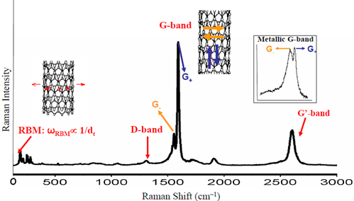
Figure 1. A typical Raman spectra for SWCNT showing important features like Radial breathing mode, D-band and G-band. Figure is taken from [9].
Raman scattering is inelastic scattering of light, i.e. scattering of light in which the photon energy changes [44]. Raman spectroscopy is to observe an inelastic scattering of light and probes the vibrational properties by measurement of the energy shift from the incident light. Resonant Raman Scattering (RRS) is a special case of Raman scattering which can give accurate information of one of the optical transition energy of any SWCNT. When a resonance condition is met, the Raman signal is strongly enhanced. In fact, in individual nanotubes, Raman scattering can only be observed with considerable signal strength when excited resonantly.
One of the unique features for SWCNT in Raman spectra is the Radial Breathing Mode (RBM) which corresponds to the coherent vibration of the carbon atoms in radial direction [9]. These features occur between frequency 120 and 350 cm-1 for SWCNT for diameter in the range 0.7nm <dt<2 nm (Fig 1). Knowing the RBM frequency for a SWCNT, its diameter can be calculated as they two are correlated through a semi-empirical equation of the form,
![]() .
.
Raman spectroscopy and Resonant Raman scattering are the most widely used characterization tools for carbon nanotubes [45]. One advantage is its abilitity to probe both semiconducting and metallic nanotubes [25]. Furthermore, unlike luminescence spectroscopy, Raman scattering requires virtually no special sample preparation. It can be performed on individual single tubes and also on samples consisting of nanotube bundles, nanotubes on various substrates, in solution or even on free - standing individual nanotubes. Therefore, it is frequently used to characterize nanotubes after growth and adjust growth conditions, and to monitor chemical reactions [45]. Because of extensive use, numerous reports on RRS given optical transition and RBM frequency (ωrbm) data are available now in literatures.
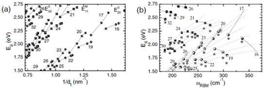
Figure 2. Chirality assignment by Fantini et al (a) Eii vs 1/dt plot from TB model with γ0 =2.9 (b) Eii vs ωrbm plot from resonance Raman spectroscopy. Solid circles and squares denote semiconducting and metallic SWCNTs, respectively. Figure is taken from [31].
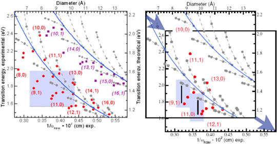
Figure 3. (Left) Kataura plot of the experimental resonance maxima vs. inverse ωrbm, compared to third-order tight-binding calculated transition energies vs nanotube diameter. Theoretical points are light grey. (Right) A shift of the assignment by an entire branch (arrows) renders an incorrect count of the number of nanotubes. Figure is taken from [5].
Herrera et al [22] characterized SWCNTs prepared by disproportion of Co over Co-Mo/Sio2 catalysts. From Raman spectroscopy they obtained gap energies of these SWCNTs using several laser excitation energies. By comparing the plot of experimental data with calculated gap energies as a function of nanotube diameter, they assigned the chirality to produced batch.
Fantini et al [31] performed resonant Raman spectroscopy to characterize a batch of SWCNTs dispersed in aqueous solution and within solid bundles, in the energy range 1.52 - 2.71 eV. They obtained electronic transition energies and the radial breathing mode frequencies for 46 different (18 metallic and 28 semiconducting) nanotubes, and made the (n,m) assignment based on the observation of geometrical patterns for Eii versus ωrbm graphs shown in Fig 2.
Thomsen et al [5] used Resonant Raman scattering of some SWCNTs to make assignment of their chiral indices. Their assignment was based on a plot of the resonance maxima for the radial breathing modes as a function of laser excitation energy versus inverse RBM frequency (ωrbm), the so-called Kataura plot (Fig 3).
Telg et al [17,32] carried out a similar resonant Raman spectroscopy but they used excitation energy in the near-infrared range from 1.15 to 1.48 eV to match with first optical transition of the produced batch of SWCNTs. They characterized them using pattern recognition from Eii versus ωrbm graphs, as shown in Fig 4.
Figure 4. Experimental Kataura plot for E11 of semiconducting SWCNTs from resonant Raman scattering (circles) and photoluminescence excitation (crosses). (+) symbols are empirical data based on photolumiscence data. Figure is taken from [32].
In another attempt by Telg et al [28], they obtained the optical transition energies, the radial breathing mode frequency, and the Raman intensity of both metallic and semiconducting tubes from resonant Raman scattering on isolated nanotubes. They unambiguously assigned the chiral index (n,m) of 50 nanotubes based solely on a third neighbor tight-binding Kataura plot.
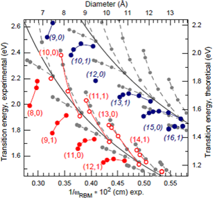
Figure 5. Chirality assignment technique shown by Maultzsch et al [25] using resonant Raman Scattering. The assignment is based on one to one correspondence between experimental (large colored circles, left and bottom axes) and theoretical (small gray circles, right and top axes) Kataura plot. Figure is taken from [25].
Maultzsch et al [25] presented a comprehensive study of the chiral-index assignment of carbon nanotubes in aqueous suspensions by resonant Raman scattering of the radial breathing mode. They determined the energies of the first optical transition in metallic tubes and of the second optical transition in semiconducting tubes for more than 50 chiral indices. They performed the pattern recognition between theoretical and experimental plots by stretching and shifting the vertical and horizontal axes of the plots until good correspondence between the experimental points and the theoretically calculated values is achieved (Fig 5). Their assignment was unique and does not depend on empirical parameters.
2.2. Rayleigh Scattering Based Technique
Rayleigh scattering is the elastic light scattering from an object that is small in diameter compared with the wavelength of the light. If the frequency of the light is in resonance with an electronic transition of the object, the scattering intensity is enhanced. This technique can probe the transition energies of both metallic and semiconducting nanotubes.
Yu et al. [46] reported Rayleigh scattering from small individual nanotube bundles on a glass substrate in dark - field geometry. A Rayleigh spectrum from Reference [46] is shown in Fig 6a. The contributions from individual nanotubes within the bundle are not resolved, but the peaks were assigned to the first transition in metallic tubes (at 650 – 700 nm) and to the third transition in semiconducting tubes (at 450 – 500 nm), as shown in Fig 6a.
Sfeir et al. [47] simultaneously determined the physical structure and optical transition energies of individual single-walled carbon nanotubes by combining electron diffraction with Rayleigh scattering spectroscopy. They directly verified the systematic changes in transition energies of semiconducting nanotubes as a function of their chirality.
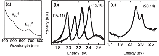
Figure 6. Rayleigh spectrums from (a) a small bundle (b) semiconducting tubes and (c) metallic tube and corresponding chirality assignments. Figure is taken from [45,46].
Lian et al [14] determined the chirality (n, m) of Raw electric-arc-produced SWNTs using optical absorption experiment. From comparisons of experimental data with theoretical predictions from electronic band theory, they assigned spectral features to the electronic transitions of their semiconducting and/or metallic SWCNTs.
Recently, Wu et al. [48] showed that Rayleigh scattering can be greatly enhanced by interface dipole enhancement effect. Generally, Single-walled carbon nanotubes (SWCNTs) illuminated by white light should appear colored due to resonance Rayleigh scattering. However, true color imaging of SWCNTs on substrate has not been reported, because of the extremely low scattering intensity of SWCNTs and strong substrate scattering. But, using the method of Wu et al. colorful SWCNTs on substrates can be directly imaged under an optical microscope by wide field supercontinuum laser illumination, which facilitates high throughput chirality assignment of individual SWCNTs. Based on their Rayleigh spectra of six individual nanotubes, the chiral indices were identified to be (16, 12) , (17, 12) , (22, 3), (13, 9), (17, 16), and (20, 6).
2.3. Photoluminescence Based Technique
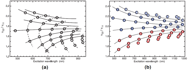
Figure 7. Comparison of excitation to emission ratio between (a) Photoluminescence result and (b)extended TB calculation for chirality assignment as used by Bachilo et al. Solid lines connect families with equal n – m values and dotted line connects 2n+m families. Correspondence between (a) and (b) gives chirality of each tube. Figure is taken from [37].
In 2002, Bachilo et al [37] and O’ Connel et al [40] independently performed two very important fluorescence spectroscopy experiments and observed band gap luminescence from SWCNTs for the first time. They observed that light absorption at photon energy equal to second optical transition is followed by fluorescence emission near first optical transition. The values of two transition energies vary with tube structure. Bachilo et al. [37] showed Photoluminescence (PL) based effective (n, m) assignment based on pattern recognition between experimental and theoretical (derived from extended tight binding model) plot of the second optical transition (excitation energy) versus the first optical transition (emission energy), as shown in Fig 7. Their method established Photoluminescence based chirality assignment of semiconducting SWCNT as an effective method for unique assignment.
Miyauchi et al. [43] performed near-infrared fluorescence measurements on single-walled carbon nanotubes (SWNTs) catalytically synthesized from alcohol under various experimental conditions (alcohol catalytic CVD method, ACCVD). They determined the chirality distribution by measuring the fluorescence emitted from separated SWNTs as a function of excitation wavelength. Compared with HiPco SWNTs, chiralities of the ACCVD sample were distributed predominantly in the higher chiral angle region, close to the armchair (n=m) structure. They observed that the tendency toward higher chiral angles was more pronounced for smaller diameter nanotubes.
Weisman et al. [39,49] presented an overview of basic and applied aspects of the fluorescent photoluminescence from single-walled carbon nanotubes (SWCNT). Their spectrofluorimetric measurements of emission intensity as a function of excitation and emission wavelengths revealed a rich pattern of peaks representing distinct (n,m) structural species. Each of these peaks can be assigned to a specific semiconducting (n,m) species by careful analysis. This spectral assignment provided a large body of precise optical transition energies for a significant range of tube diameters and chiralities. They showed that Fluorimetry can offer a powerful method for determining the (n,m) composition of mixed nanotube samples. They also discussed instrumental methods for such fluorimetric analysis.
2.4. A Comparison of Three Main Techniques Mentioned Above
In this section, we will present a brief comparison of these three main techniques discussed above, namely, Raman scattering, Rayleigh scattering and Photoluminescence based chirality assignment techniques. Relative advantages and disadvantages of each of these techniques will be also highlighted.
The advantage of photoluminescence excitation spectroscopy based technique for chirality assignment of SWCNTs compared with Raman scattering is that it can be very fast and does not require the laborious analysis necessary for extracting Raman resonance profiles. Furthermore, a broad-band white light source is usually sufficient for excitation, in contrast to tunable lasers required for resonance Raman spectroscopy. On the other hand, photoluminescence probes only semiconducting nanotubes, in contrast to Raman and Rayleigh scattering [45].
The advantage of Rayleigh scattering based technique is, it can probe the transition energies of a nanotube independent of the tube’s metallic or semiconducting character, combining in principle some advantages from Photoluminescence and Raman spectroscopy, i.e. a rather fast experiment and the access to the transitions in metallic nanotubes. On the other hand, in this technique the signal strength is typically very low, requiring a bright light source and a sample geometry in which possible scattering background from nearby scatterers is almost entirely suppressed [45].
Resonant Raman Scattering (RRS) is quite reliable, straight-forward and hence most widely used for chiral index assignment. The advantage of Raman scattering over photoluminescence is that it can identify both metallic and semiconducting nanotubes [25,50]. Besides, unlike Photoluminescence spectroscopy, Raman scattering requires virtually no special sample preparation. It can be performed on individual single tubes and also on samples consisting of nanotube bundles, nanotubes on various substrates, in solution or even on free - standing individual nanotubes. Moreover, photoluminescence are sometimes destructive, since the sample has to undergo a separation procedure, which is irreversible and till now there is no way to completely remove the surfactant [40,50]. Also, in semiconducting nanotubes Raman spectroscopy can be performed in resonance with the second optical transition, which is in the visible energy range. Thus, no infrared-sensitive spectrometers and detectors are needed [25]. RRS provides two important pieces of information: one of the optical transition energies (Eii) and the RBM frequency (ωrbm). This ωrbm then gives diameter dt as they two are inversely related through a semi-empirical relation [6,26,27,37,51,52]. Because the (Eii , ωrbm) pair is unique for each SWCNT, proper structural assignment can be made using a prior theoretical model for (Eii, ωrbm) to (n, m) transformation [31]. Earlier approach was to plot all Eii versus dt (from ωrbm) to form an experimental kataura plot which is mapped with an existing theoretical kataura plot to give one-to-one correspondence for each chirality [22,27]. Unfortunately, the uniqueness of this transformation may be hampered in this process by possible error involved in empirical calculation of dt from ωrbm. So, a smarter method was proposed later by many authors where all Eii are plotted directly against corresponding ωrbm [31,32] or inverse ωrbm [5,25,28] (instead of dt) and compared with a theoretical plot of (Eii, ωrbm) or (Eii, 1/ωrbm). Then pattern recognition between two plots is performed by stretching and shifting the vertical and horizontal axes of the plots until good correspondence between the experimental points and the theoretically calculated values is achieved [5,25,28]. By this process, assumption of empirical parameters for calculating dt from ωrbm can be avoided and possible theoretical or experimental error can be neutralized within a limit. This pattern recognition finally gives a unique one-to-one correspondence for each chiral index (n, m).
Though different methods of SWCNT chirality assignment using different spectroscopic experiments are discussed above, in principle they bear some similarities. All of them follow a laborious mapping of observed properties of produced batch of SWCNTs with an existing theoretical plot depicting same properties to find one-to-one correspondence of chirality. So, all these process need to go through some kind of pattern recognition between experimental and theoretical data which requires a prior theoretical or empirical graphical plot to make final assignment [25,31]. Moreover, Pattern recognition is possible only if the Raman spectrum shows a set of different RBMs. This is only the case for samples containing different kinds of nanotubes, i.e. produced as ensembles of nanotubes. When all observed Raman spectra show only one RBM, e.g. for an isolated tube or when the sample contains only one kind of chiral indices (n, m), there is no scope for pattern recognition. In such case, quality of the assignment fully depends on the chosen theoretical plot and may lead to ambiguity [50].
2.5. Other Techniques
In this section, we briefly discuss other characterization methods for carbon nanotubes. At first, some unconventional techniques reported by some authors will be presented.
Li et al. [53] observed strain-induced band gap shifts by optical spectroscopy in single-walled carbon nanotubes (SWCNTs) that depend strongly on the chiral angle. They generated uniaxial and torsional strains by changing the environment surrounding the SWCNTs, using the surrounding D2O ice temperature or the hydration state of a wrapping polymer. They used these methods as diagnostic tools to determine the quantum number q and examine chiral vector indices for specific nanotubes.
Ohno et al. [54] proposed a possibility of chirality assignment of individual single-walled carbon nanotubes in nanotube field-effect transistors (FETs) by micro-photocurrent spectroscopy. They fabricated the nanotube FETs by utilizing position-controlled nanotube growth technique using alcohol chemical vapor deposition. Photocurrent signal that originated from a single-walled carbon nanotube was obtained by using microscopic optical measurement system. A peak was observed at 1.73 eV in the photocurrent excitation spectrum. This corresponds to optical absorption by van Hove singularity of the nanotube with a diameter of ~ 2 nm. Chirality of the nanotube which they observed in the nanotube FET was assigned to be (18, 10) by comparing the experimental results with theoretical calculation.
Besides, SWCNT imaging techniques are sometimes used for chirality assignment of some specific SWCNTs. Imaging techniques like scanning probe microscopy or electron diffraction can directly visualize the nanotube structure. This is unlike any optical methods mentioned in previous sections where optical spectroscopy is used to probe certain properties of the tube from which the chiral index is deduced with the help of theoretical predictions.
Electron diffraction is one of such tools for (n, m) determination [45,47,55,56]. The diffraction pattern of a single - walled carbon nanotube consists of two structures with hexagonal symmetry, which are rotated against each other. They arise from the front and back wall of the nanotube. The chiral angle of the nanotube can be derived from the angle between them.
The advantage of electron diffraction is its reliability, in particular, the chiral indices of large - diameter tubes are identified. This appears to be difficult in Raman scattering and Photoluminescence, as the RBM frequencies and optical energies are too close within the same Kataura branch for diameters above 2 nm. The disadvantage is, only one nanotube can be probed at a time, i.e. electron diffraction cannot be applied to nanotube ensembles. Besides, electron diffraction requires special sample preparation compared with optical measurements and the nanotube might be damaged or even destroyed by the electron beam [45].
Scanning tunneling microscopy (STM) probes the surface structure of carbon nanotubes with atomic resolution, which in principle permits determination of the chiral index [19-21]. High-resolution transmission electron microscopy (HRTEM) is suited to measure quickly the diameter of a nanotube [18]. Atomic force microscopy (AFM) and scanning electron microscopy (SEM) are both standard methods to characterize nanotubes on a substrate with respect to their shape and location. They are fast and usually image larger sample areas than STM [45].
It is important to note that Electron diffraction, STM, HRTEM, AFM, SEM - all these are mainly for imaging purposes rather than characterization of optical or electronic properties. These imaging techniques are used for chirality assignment of SWCNTs only in some specific cases.
2.6. Some Most Recent and Improved Techniques
In recent years, there have been some important developments in characterization methods for carbon nanotubes. We will present here some of those most recent reports.
K. Liu et al. [57] reported high-throughput real-time optical imaging and broadband in situ spectroscopy of individual carbon nanotubes on various substrates and in field effect transistor devices using polarization-based microscopy combined with supercontinuum laser illumination. their technique enables the complete chirality profiling of hundreds of individual carbon nanotubes, both semiconducting and metallic, on a growth substrate. Their optical images showed high contrast for all individual nanotubes from which they identifed that the nanotubes have chiralities of (20,6), (22,16) and (26,22). These are semiconducting, metallic and semiconducting nanotubes with diameters of 1.8, 2.6 and 3.3 nm, respectively.
Roch et al. [58] presented an experimental investigation of the optical spectra of single walled carbon nanotubes (SWCNT) at temperatures up to 1273 K. Their investigation gives insights into the electronic structure of metallic and semiconducting SWCNT at different temperatures by measuring the shift of the first and second optical transition of semiconducting SWCNTs and first optical transition of metallic SWCNTs with optical absorption spectroscopy. They observed a decrease of the transition energies in both metallic and semiconducting SWCNT with increasing temperature. Furthermore, they performed calculation of the average exciton binding energy (80–90 meV) in metallic SWCNT. They demonstrate that the optical absorption spectroscopy can be an effective tool for characterization of the electrical properties and structure of SWCNT.
Inoue et al. [59] evaluated the populations and lengths of SWCNTs with different chiralities (n,m) independently utilizing the aligned morphology of single-walled carbon nanotubes (SWCNTs) grown on crystal quartz substrates together with systematic Raman mapping measurements. Chiralities of SWCNTs were assigned on a one-by-one basis by comparing radial breathing mode frequencies with the Kataura plot. The SWCNT lengths were determined by Raman mapping and/or scanning electron microscopy. Both the populations and lengths of the SWCNTs grown in their study with a diameter of 1.14 to 1.29 nm showed no clear dependence on their chiral angles.
Wu et al. [48] showed very recently that Rayleigh scattering can be greatly enhanced by interface dipole enhancement effect. Using the method proposed by Wu et al., colorful SWCNTs on substrates can be directly imaged under an optical microscope by wide field supercontinuum laser illumination, which facilitates high throughput chirality assignment of individual SWCNTs.
These recent reports show good potential in chirality determination of SWCNTs. However, we need to wait more to explore the complete potentials of these new methods.
3. Conclusion
Here, we have discussed the importance of determining the chirality of any single wall carbon nanotube. We have presented a review on some important theoretical and experimental methods for determination of chirality of SWCNTs. Resonant Raman Scattering (RRS), Rayleigh scattering and Photoluminescence (PL) excitation have been presented as the mainstream tools for nondestructive chirality characterization. We presented a summary of these three main techniques used by different researchers for chirality assignment of metallic and semiconducting SWCNTs. We also discussed some old or less conventional alternative techniques for chirality assignment of SWCNTs. Finally, we presented some most recent and potential works on chirality determination method. We highlighted the advantage and limitations of each of the existing techniques for chirality assignment of SWCNTs and gave an overall comparison between them. This review can help the researchers to get a brief but all-inclusive idea on various chirality determination techniques from past to present.
References
- V. N. Popov, "Carbon nanotubes: properties and application", Materials Science and Engineering R, 43, pp. 61–102, 2004.
- T. W. Odom, J. L. Huang, P. Kim, and C. M. Lieber, "Structure and Electronic Properties of Carbon Nanotubes", J. Phys. Chem. B, 104, pp.2794-2809, 2000.
- N. Hamada, S. Sawada, and A. Oshiyama, "New one-dimensional conductors: graphitic microtubules," Phys. Rev. Lett., Vol.68, No.10, p. 1579-1581, 1992.
- Y. Lim, K. Yee, J. Kim, E. H. Hároz, J. Shaver, J. Kono, S. K. Doorn , R. H. Hauge , R. E. Smalley, "Chirality Assignment of Micelle-Suspended Single-Walled Carbon Nanotubes Using Coherent Phonon Oscillations", Journal of the Korean Physical Society, Vol. 51, No. 1, pp. 306-311, 2007.
- C. Thomsen, H. Telg, J. Maultzsch and S. Reich, "Chirality assignments in carbon nanotubes based on resonant Raman scattering", phys. stat. sol. (b) 242, No. 9, pp.1802–1806, 2005.
- M. S. Strano, S. K. Doorn, E. H. Haroz, C. Kittrell, R. H. Hauge and R. E. Smalley, "Assignment of (n, m) Raman and Optical Features of Metallic Single-Walled Carbon Nanotubes", Nano Lett., Vol.3, No.8, pp. 1091-1096, 2003.
- J. W. Mintmire and C. T. White, "Universal density of states for carbon nanotubes", Phys. Rev. Lett., Vol. 81, No.12, 1998.
- S. Reich and C. Thomsen, "Chirality dependence of the density-of-states singularities in carbon nanotubes", Phys. Rev. B, Vol 62, No. 7, 2000.
- M.S. Dresselhausa, G. Dresselhausc, A. Jorio, A.G. Souza Filho, R. Saito, "Raman spectroscopy on isolated single wall carbon nanotubes", Carbon, 40, pp.2043–2061, 2002.
- T. Tanaka, H. Jin, Y. Miyata, S. Fujii, H. Suga, Y. Naitoh, T. Minari, T. Miyadera, K. Tsukagoshiand H. Kataura, "Simple and Scalable Gel-Based Separation of Metallic and Semiconducting Carbon Nanotubes", Nano Lett., 9 (4), pp 1497–1500, 2009.
- R. Krupke, F. Hennrich, H. von Lohneysen and M. M. Kappes, "Separation of metallic from semiconducting single-walled carbon nanotubes", Science, 301, pp.344–347, 2003.
- R. Voggu, K. V. Rao, S. J. George and C. N. R. Rao, "A Simple Method of Separating Metallic and Semiconducting Single-Walled Carbon Nanotubes Based on Molecular Charge Transfer", J. Am. Chem. Soc., 132 (16), pp 5560–5561, 2010.
- S. Ghosh and C. N. R. Rao, "Separation of Metallic and Semiconducting Single-Walled Carbon Nanotubes Through Fluorous Chemistry", Nano Res 2, pp.183-191, 2009.
- M. Mattsson, A. Gromov, S. Dittmer, E. Eriksson, O. A. Nerushev, E. E. B. Campbell, "Dielectrophoresis-induced separation of metallic and semiconducting single-wall carbon nanotubes in a continuous flow microfluidic system", Journal of nanoscience and nanotechnology, vol. 7, No. 10, pp.3431-3435, 2007
- F. Hennrich, K. Moshammer, M M Kappes, "Separation of metallic from semiconducting single walled carbon nanotubes by size exclusion chromatography", Nature Nanotechnology, Vol. 344, Issue c, pp.76128-76128, 2009.
- Feng Ye, "Metallic-semiconducting separation of single wall carbon nanotubes and their application to electronic devices", Ph.D thesis in Materials Science, University of Tsukuba, Japan, February 2011.
- H. Telg, J. Maultzsc, S. Reich, F. Hennrich, and C. Thomsen, "Raman intensities of the first optical transitions in carbon nanotubes", Phys. stat. sol. (b) 243, No. 13, pp.3181–3185, 2006.
- C. Qin and L.M. Peng, "Measurement accuracy of the diameter of a carbon nanotube from TEM images", Phys. Rev. B 65, 155431, 2002.
- M. Ge, and K. Sattler, "Scanning tunneling microscopy of single-shell nanotubes of carbon", Appl. Phys. Lett., 65, 2284, 1994.
- L. C. Venema, V. Meunier, Ph. Lambin, and C. Dekker, "Atomic structure of carbon nanotubes from scanning tunneling microscopy", Phys. Rev. B 62, pp.2991-2996, 2000.
- T. W. Odom, J. L. Huang and C. M. Lieber, "STM studies of single-walled carbon nanotubes", J. Phys.: Condens. Matter 14, R145–R167, 2002.
- J. E. Herrera, L. Balzano, F. Pompeo and D. E. Resasco, "Raman characterizatiuon of Single wall nanotubes of various diameters obtained by catalytic disproportionation of CO", J. Nanosci. Nanotech, Vol. 3, No. 1, 2003.
- R. B. Weisman and S. M. Bachilo, "Dependence of optical transition energies on structure for single-walled carbon nanotubes in aqueous suspension: an empirical kataura plot," Nano Lett., Vol.3, No.9, pp. 1235-1238, 2003.
- Z. Wang, H. Zhao, and S. Mazumdar, "Quantitative calculations of the excitonic energy spectra of semiconducting single-walled carbon nanotubes within a-electron model", Phys. Rev. B 74, 195406, 2006.
- J. Maultzsch, H. Telg, S. Reich, and C. Thomsen, "Radial breathing mode of single-walled carbon nanotubes Optical transition energies and chiral-index assignment", Phys. Rev. B 72, 205438, 2005.
- S.K. doorn, D.A. Heller, P.W. Barone, M.L. Usrey, M.S. Strano, "Resonant Raman excitation profiles of individually dispersed single walled carbon nanotubes in solution", Appl. Phys. A 78, p.1147–1155, 2004.
- Z. Yu and L. E. Brus, "(n, m) Structural Assignments and Chirality Dependence in Single-Wall Carbon Nanotube Raman Scattering", J. Phys. Chem. B, 105, pp.6831-6837, 2001.
- H. Telg, J. Maultzsch, S. Reich, F. Hennrich and C. Thomsen, "Chirality Distribution and Transition Energies of Carbon Nanotubes" Phys. Rev. Lett., Vol. 93, No. 17, 2004.
- A. Jorio, A. P. Santos, H. B. Ribeiro, C. Fantini, M. Souza, J. P. M. Vieira, C. A. Furtado, J. Jiang, R. Saito, L. Balzano, D. E. Resasco and M. A. Pimenta, "Quantifying carbon-nanotube species with resonance Raman scattering" Phys. Rev. B 72, 075207, 2005.
- H. Telg, J. Maultzsch, S. Reich, F. Hennrich and C. Thomsen, "Raman excitation profiles for the (n1, n2) assignment in carbon nanotubes" AIP Conf. Proceedings, Vol. 723, Issue 1, p.330, 2004.
- C. Fantini, A. Jorio, M. Souza, M. S. Strano, M. S. Dresselhaus and M. A. Pimenta, "Optical Transition Energies for Carbon Nanotubes from Resonant Raman Spectroscopy: Environment and Temperature Effects", Phys. Rev. B, Vol. 93, No. 14, 2004.
- H. Telg, J. Maultzsch, S. Reich and C. Thomsen, "Resonant-Raman intensities and transition energies of the E11 transition in carbon nanotubes", Phys. Rev. B 74, 115415, 2006.
- Y. Lian, Y. Maeda, T. Wakahara, T. Akasaka, S. Kazaoui, N. Minami, N. Choi and H. Tokumoto, "Assignment of the Fine Structure in the Optical Absorption Spectra of Soluble Single-Walled Carbon Nanotubes", J. Phys. Chem. B, 107, 12082-12087, 2003.
- A. Hagen and T. Hertel, "Quantitative Analysis of Optical Spectra from Individual Single-Wall Carbon Nanotubes", Nano letters, Vol. 3, No. 3, pp. 383-388, 2003.
- M. Namkung, P. A. Williams, C. D.Mayweather, B. Wincheski, C. Park,; Namkung, S. Juock, "Chirality Characterization of Dispersed Single Wall Carbon Nanotubes" NASA, 2005 MRS Spring Meeting; San Francisco, CA; United States, 28 Mar. - 1 Apr. 2005.
- S. Berciaud, L. Cognet, P. Poulin, R. Bruce Weisman, and B. Lounisa, "Absorption spectroscopy of individual single-walled carbon nanotubes", Nano Lett., 7 (5), pp.1203–1207, 2007.
- Bachilo S. M., Strano M. S., Kittrell C., Hauge R. H., Smalley R. E., Weisman R. B., "Structure-Assigned Optical Spectra of Single-Walled Carbon Nanotubes", Science, Vol 298 No. 5602, pp. 2361, 2002.
- J. Lefebvre, S. Maruyama and P. Finnie, "Photoluminescence: science and applications", Topics in Applied Physics,Vol. 111, pp.287-319, 2008.
- R. B. Weisman, "Fluorimetric characterization of single-walled carbon nanotubes", Anal. Bioanal. Chem. 396, 1015–1023, 2010.
- M. J. O'Connell, S.M. Bachilo, C.B. Huffman, V.C. Moore, M.S. Strano, E.H. Haroz, K.L. Rialon, P.J. Boul, W.H. Noon, C. Kittrell, J. Ma, R.H. Hauge, R.B. Weisman, and R.E. Smalley, "Band Gap Fluorescence from Individual Single-Walled Carbon Nanotubes", Science 297, pp.5581-5593, 2002.
- D. A. Tsyboulski1, J. D. R. Rocha, S. M. Bachilo1, L. Cognet and R. B. Weisman,"Structure-Dependent Fluorescence Efficiencies of Individual Single-Walled Carbon Nanotubes", Nano Lett.,7(10), pp.3080-5, 2007.
- M. Jones, C. Engtrakul, W. K. Metzger, R. J. Ellingson, A. J. Nozik, M. J. Heben, and G. Rumbles, "Analysis of photoluminescence from solubilized single-walled carbon nanotubes", Phys. Rev B, 71, 115426, 2005.
- Y. Miyauchi, S. Chiashi, Y. Murakami, Y. Hayashida, S. Maruyama, "Fluorescence spectroscopy of single-walled carbon nanotubes synthesized from alcohol", Chem. Phys. Lett., Vol. 387, Issues 1–3, pp.198–203, 2004.
- T. S. Jespersen, "Raman Scattering in Carbon Nanotubes", M.Sc. Thesis, Faculty of Science, University of Copenhagen, 2003.
- J. Maultzsch, C. Thomsen, "Characterization of Carbon Nanotubes by Optical Spectroscopy, Advanced Micro and Nanosystems", Carbon Nanotube Devices, Vol. 8., Edited by Christofer Hierold, Verlag GmbH and Co. KGaA, Weinheim, Berlin, Germany, 2008.
- Z. Yu, L. E. Brus, "Rayleigh and Raman scattering from individual carbon nanotube bundles", J. Phys. Chem. B, 105, p.1123, 2001.
- M. Y Sfeir., T. Beetz, F Wang, L. Huang, X. M. H Huang., M. Huang, J. Hone, S. O’Brien, J. A Misewich, T. F. Heinz, L. Wu, Y. Zhu, L. E. Brus, "Optical Spectroscopy of Individual Single-Walled Carbon Nanotubes of Defined Chiral Structure", Science, Vol. 312, April 2006.
- W. Wu et al., "True-color real-time imaging and spectroscopy of carbon nanotubes on substrate by enhanced Rayleigh scattering", Nano Res., Just Accepted Manuscript, DOI: 10.1007/s12274-015-0779-x, April 2015.
- R. B. Weisman, "Fluorescence Spectroscopy of Single-Walled Carbon Nanotubes", Applied Physics of Carbon Nanotubes, Editors: S. V. Rotkin, S. Subramoney, Chapter: NanoScience and Technology, pp. 183-202, 2005.
- H. Telg, "Raman studies on individual nanotubes and nanotube ensembles –vibrational properties and scattering efficiencies", Ph.d thesis, Physics, Institute für Festkörperphysik, Berlin, 2009.
- J. L. Sauvajol, E. Anglaret, S. Rols, L. Alvarez, "Phonons in single wall carbon nanotube bundles", Carbon, 40, 1697, 2002.
- U. D. Venkateswaran, A. M. Rao, E. Richter, M. Menon, A. Rinzler and R. E. Smalley, "Probing the single-wall carbon nanotube bundle: Raman scattering under high pressure", Phys. Rev. B, Vol. 59, No. 16, 1999.
- L. J. Li, R. J. Nicholas, R. S. Deacon and P. A. Shields, "Chirality assignment of single-walled carbon nanotubes with strain", Phys. Rev. Lett. 93(15):156104, 2004.
- Y Ohno, S Kishimoto, T Mizutani, T Okazaki and H Shinohara, "Chirality assignment of individual single-walled carbon nanotubes in carbon nanotube field-effect transistors by micro-photocurrent spectroscopy", App Phys Lett., Vol 84, No 8, 2004.
- J. C. Meyer, M. Paillet, G. S. Duesberg, S. Roth, "Electron diffraction analysis of individual single - walled carbon nanotubes" Ultramicroscopy , 106, p.176, 2006.
- M. Gao, J. M. Zuo, R. D. Twesten, I. Petrov, L. A. Nagahara, R. Zhang, "Structure determination of individual single - wall carbon nanotubes by nanoarea electron diffraction", Appl. Phys. Lett. , 82, p.2703, 2003.
- Kaihui Liu et al., "High-throughput optical imaging and spectroscopy of individual carbon nanotubes in devices", Nature Nanotechnology 8, pp. 917–922, 2013.
- A Roch, L Stepien, T Roch, I Dani, C Leyens, O Jost and A Leson, "Optical absorption spectroscopy and properties of single walled carbon nanotubes at high temperature", Synthetic Metals 197, pp.182–187, 2014.
- T. Inoue, D. Hasegawa, S. Chiashia and S. Maruyama, "Chirality analysis of horizontally aligned single walled carbon nanotubes: decoupling populations and lengths", J. Mater. Chem. A, 3, 15119, 2015.


