
Journal of Nanoscience and Nanoengineering, Vol. 1, No. 2, August 2015 Publish Date: Aug. 13, 2015 Pages: 84-95
Beyond the Basic Tight Binding Model to Calculate Optical Transition Energies of SWCNT
G. R. Ahmed Jamal1, *, S. M. Mominuzzaman2
1Department of Electrical and Electronic Engineering, University of Asia Pacific, Dhaka, Bangladesh
2Department of Electrical and Electronic Engineering, Bangaldesh University of Engineering and Technology, Dhaka, Bangladesh
Abstract
The one-dimensionality of the Single Wall Carbon Nanotubes (SWCNT) give rise to 1D sub-bands in nabnotu be density of states. The tight-binding (TB) model has been widely used for modeling electronic band structure of SWCNT due to its simplicity. A number of recent optical spectroscopic experiments reveal that TB model fails to give accurate quantitative and qualitative description of different optical transition energies in SWCNTs. Hence, many authors tried to improve this model through different approaches so as to extend the capacity of basic TB model to predict different optical transition energies in SWCNTs. Some tried to calculate the band structure from first principle calculations. Others proposed empirical models to fit the experimental results. This work presents a review of some important previous research works that proposed improved TB models, empirical models or first principle based models to overcome the limitation of basic TB model in calculating different optical transitions of SWCNTs. The advantage and limitation of each of these approaches are also highlighted in this work.
Keywords
SWCNT, Density of State, Optical Transition Energy, Tight Binding Model, Chiral Index
Received: July 9, 2015
Accepted: July 31, 2015
Published online: August 13, 2015
@ 2015 The Authors. Published by American Institute of Science. This Open Access article is under the CC BY-NC license. http://creativecommons.org/licenses/by-nc/4.0/
1. Introduction
Carbon Nanotubes are one of the allotropes of carbon having unique one-dimensional nanostructure and extraordinary electronic, optical, mechanical and chemical properties. Electronic and optical properties of single-wall carbon nanotubes (SWCNT) are directly associated with their geometrical structures [1,2] which are uniquely specified by a pair of chiral index (n, m). A SWCNT (n, m) will be metallic if its n-m = 3k (k is integer), i.e. mod (n-m, 3) = 0 and it will be semiconducting if its n-m ≠ 3k, i.e. mod (n-m, 3) = 1 or 2 [3]. This relation gives two types of semiconducting SWCNTs, mod 1 type and mod 2 types.
The one-dimensionality of the nanotubes gives rise to 1D sub-bands instead of one wide electronic energy band in nanotube density of states (DOS), as shown in Fig 1. Each SWCNT (n, m) has a unique set of interband transition energies Eii denoting the energy differences between the i-th conduction and valence bands and optical transitions can only occur between these mirror sub-bands [1,2,4,6]. These singularities are unique feature of nanotubes and also primarily responsible for many distinguished electronic and optical properties of SWCNTs.
Many applications of semiconducting SWCNT require prior information of these optical transition energies (specially, the bandgap energy). Hence, accurate calculation of their optical transition energies from a theoretical model is a necessity. The tight-binding (TB) model of π-bands of graphene using the zone-folding approximation has been widely used for modeling electronic band structure of single-wall carbon nanotube (SWCNT) due to its simplicity, low computational cost, and some qualitative agreement with experimental results [7-9]. TB model with the nearest-neighbor approximation provides following simple expression to calculate optical transitions of a semiconducting nanotubes [1,2,10]:
![]() (1)
(1)
Where, ![]() is the nearest-neighbor hopping parameter,
is the nearest-neighbor hopping parameter, ![]() Å is carbon-carbon bond length,
Å is carbon-carbon bond length, ![]() is nanotube diameter in nm, given by
is nanotube diameter in nm, given by ![]() and j is an integer. Eiicorresponds to the first, second, third, fourth…… interband transitions (E11S, E22S, E33S, E44S….) of semiconducting SWCNT when j = 1, 2, 4, 5… respectively, and to the first and second interband transition (E11M, E22M ) of metallic SWCNT when j = 3 and 6, respectively. This inverse proportional trend of transition energies with SWCNT diameter, given by Eqn. (1), is also observed from the Kataura plot [11,12] and from other optical spectroscopic experiments [6,13].
and j is an integer. Eiicorresponds to the first, second, third, fourth…… interband transitions (E11S, E22S, E33S, E44S….) of semiconducting SWCNT when j = 1, 2, 4, 5… respectively, and to the first and second interband transition (E11M, E22M ) of metallic SWCNT when j = 3 and 6, respectively. This inverse proportional trend of transition energies with SWCNT diameter, given by Eqn. (1), is also observed from the Kataura plot [11,12] and from other optical spectroscopic experiments [6,13].
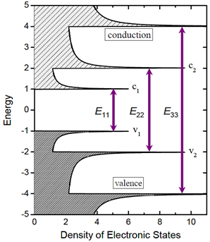
Figure 1. Schematic of density of states for a semiconducting single-walled carbon nanotube according to simple band theory model. Allowed optical transitions are illustrated as vertical arrows.
Here, the first optical transition (E11) is the bandgap of semiconducting SWCNTs and the second optical transition (E22)facilitates various optical spectroscopic experiments, as it falls within visible energy range. Also, for photo absorption, first two optical transitions are mainly considered. Hence, E11 and E22 of semiconducting SWCNTs are more significant than other transitions and are of more interest [14].
The qualitative agreement of Eqn (1) with experimental results is good [11], but it fails to predict optical transition energies with quantitative accuracy to the limit that it underestimates and overestimates first and second optical transition energies of semiconducting SWCNTs (E11S, E22S) around 25% even with the best choice of ![]() as a fitting constant parameter [12]. Equation (1) also fails to reflect relative difference between mod 1 and mod 2 type semiconducting SWCNTs for odd transitions (like, E11) and even transitions (like, E22) with comparable diameter [13] and gives incorrect ratio of first two optical transitions [14], as observed from various optical spectroscopic experiments.
as a fitting constant parameter [12]. Equation (1) also fails to reflect relative difference between mod 1 and mod 2 type semiconducting SWCNTs for odd transitions (like, E11) and even transitions (like, E22) with comparable diameter [13] and gives incorrect ratio of first two optical transitions [14], as observed from various optical spectroscopic experiments.
These disagreements of Eqn (1) are attributed to many factors. One major factor is nanotube ‘curvature effect’ induced band structure deviation from simple π-orbital graphene picture [15-18]. Other factors are ‘chirality effect’ [19], ‘trigonal warping effect’ [13,15,20] and many body effect (electron-electron interaction) comprising self-energy and exitonic effect [21-26].
Considering the limitations of basic TB model, several authors [7,9,12,14,16,18,20,26,39] tried to improve basic TB model calculation of electronic band structure of SWCNTs so as to fit it with various experimental observations. Some of them just extended simple π-band model to get better calculation. Some proposed modified or alternative model within or beyond the TB model approach and showed improved calculation using that. Some of them tried to improve TB model Eqn (1) by including extra terms with it which they deduced theoretically or empirically. Some took pure empirical approach and proposed model independent empirical equations.
The objective of this work is to present a review of those efforts that proposed either an improved basic TB model or devised empirical models to calculate electronic band structure of SWCNTs in a better way. This work will also highlight the limitations of each of those models.
2. Improved Models to Calculate Optical Transition of SWCNTs
2.1. Improved Tight Binding Models
2.1.1. Non-Orthogonal Tight-Binding Model
Popov et al [16] studied the effects of nanotube curvature on the structure, electronic and optical properties of isolated single-walled carbon nanotubes within a symmetry-adapted non-orthogonal tight-binding model using 2s and 2p electrons of carbon. Their symmetry-adapted scheme allows significant reduction of the size of matrix eigenvalue problem for the electrons for any nanotube type. This simplification enables calculation of the electronic band structure of nanotubes with a very large number of atoms in the unit cell. By considering the curved wall of the nanotubes in their model, they could improve the predictions of the optical transition energies. This theory applies on the transition energies of all nanotubes (n, m). The transition energies for the optimized structure within this model were found to agree well with the available ab initio data for a few nanotube types. On the other hand, the derived transition energies deviate widely from π-band tight-binding model calculation, especially for small radius tubes.
The calculated transition energies from non-orthogonal TB for the three tubes (5, 0), (3, 3) and (4, 2) are 1 ev, 2.9 eV, and 1.96 eV, respectively, which correspond well to the ab initio LDA results 1.2, 2.9 and 1.9eV, respectively.
Figure 2. Calculated optical transition energies within the non-orthogonal TB model (filled symbols) for all nanotubes with radii between 0.2 nm and 0.8 nm and Nc (number of atoms/unit cell))<400 in comparison with π-TB results for transfer integral γ0= 2.75eV (open symbols). Figure is taken from [16].
The band gaps derived from this model for optimized zigzag tubes (6, 0), (9, 0), (12, 0) and (15, 0) are 0.45, 0.127, 0.046 and 0.025eV respectively. For comparison, the results for the gaps of π-TB models with parameters fitted to experimental data are 0.20, 0.07eV, for tubes (6, 0) and (9, 0). Corresponding ab initio LDA results shows tube (6, 0) to be metallic and gives 0.093, 0.078 and 0.028 eV for tubes (9, 0), (12, 0) and (15, 0). The gaps measured by scanning tunneling spectroscopy for tubes (9, 0), (12, 0) and (15, 0) are 0.080, 0.042 and 0.029 eV.
As an overall comparison, for very small diameter of ≈ 0.4 nm, the π-TB results overestimate the non-orthogonal TB transition energies up to ≈ 0.5eV. For moderate diameter, the π-TB results are upshifted by about ≈0.1eV. By ab initio LDA calculations similar shifts of ≈0.1eVwere obtained for nanotubes with radii in the range 5Å<R<7.5Å.
Limitation: It has been shown that the calculated E11 and E22 for nanotubes in the diameter range from d = .6 to 1.2 nm agree well with experimental data after a uniform upshift of the calculated values by 300 meV [16]. However, at larger diameters the 300 meV up shifted values from the non - orthogonal thight-binding model seem to be slightly higher than empirical relations based on experimental data would predict [40].
Although their theory considers changes in the electronic bandstructure due to the curved walls, it neglects deviations from the idealized atomic structure due to curvature induced weakening of the bonds [41]. This relaxation of the atomic structure can be addressed by ab-initio calculations. However, for chiral nanotubes with unit cells containing more than 100 atoms, this technique is too time consuming to be applied to all (n, m) [41].
2.1.2. TB sp3s* Model
Cao et al [27] presented a TB sp3s*model for first neighboring interactions to calculate the electronic band structure only in zigzag (n, 0) SWCNTs with n= 6, 7, 8, 9. They used The 2s, 2px, 2py, 2pz, and s* orbitals of each carbon atom as the basis set for expressing the tightbinding model, and took into account the inter atom interaction between neighboring sites. With their sp3s*TB model, they calculated band gaps of (6, 0), (7,0), (8,0) and (9, 0) as .05 eV, 1.05 eV, 1.19 eV and .07 eV, respectively. Corresponding ab initio LDA results are -.83 eV, .09 eV, .62 eV and .17 eV, respevtively. Their calculation shows that (6, 0) and (9, 0) tubes are narrow-gap semiconductors, while they are predicted to be metallic from previous works. They attributed this difference to the excited s* states coupling with the anti-bonding p-like conduction states as the graphite sheet is rolled into a nanotube.
Limitation: The limitation of their approach is, it contradicts the ab initio result with which they compared their result. It predicts (6, 0) tube a narrow-gap semiconductors whereas many other independent report confirmed it as metallic. Moreover, their proposed model adresssed zigzag (n, 0) tubes only. So, applicability and accuracy of this model in calculating band structure of chiral tubes cannot be known.
2.1.3. Extended TB Model Considering up to Third Nearest Neighbors
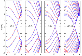
Reich et al [9] studied the band structure of isolated and bundled carbon nanotubes on the basis of ab initio calculations and discussed the limits of the graphene π-band TB model in describing the carbon nanotube bands. They showed that, if third-nearest neighbors are included, the tight-binding approximation quite accurately describes first principles results over the entire Brillouin zone. They made the TB parametrization for the graphene taking into account the interaction to third neighbors and fitting the graphene band structure to the calculated TB parameters. They used a different SIESTA basis to show the TB parameter dependence of the chosen basis. With such parametrization they showed that the TB model for third nearest neighbors describes properly the π and π*graphene bands. The electronic structure for SWNTs of large diameter within this model, is in very good agreement with ab initio calculations. They calculated band structure of (10,10) and (19,0) tubes using their model and corresponding result closely matched with ab initio calculation wheras differed significantly from nearest neighbor TB model.
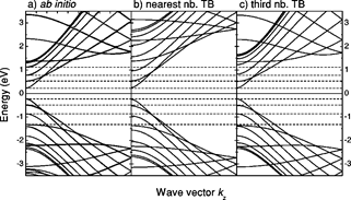
Figure 3. Band structure of a (19,0) zigzag nanotube. (a) Ab initio calculation. (b) Nearest-neighbor tight-binding calculation with γo= 2.7 eV. (c) Third-nearest-neighbor tight-binding calculation with parameters obtained from a fit to the optical energy range. The dashed lines denote ab initio calculated energies of the singularities in the density of states. Figure is taken from [9].
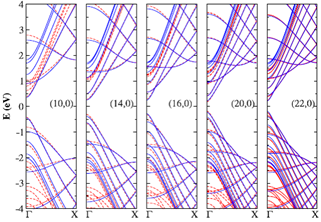
Correa et al [7] presented a similar parametrized tight-binding (TB) model to calculate the band structure of single-wall carbon nanotubes (SWNTs). On the basis of ab initio calculations, they fited the band structure of nanotubes of different diameters with results obtained with an orthogonal TB model to third neighbors, which includes the effects of orbital hybridization by means of a reduced set of parameters.
Limitation: Though TB model with third nearest neighbor give much more improved calculation of the band structure and corresponding optical transition energies, but for the inclusion of curvature effects, this model involve too many TB parameters to give an adequate description in a wide range of energies. Inclusion of both hopping and overlap integrals up to third nearest neighbors requires higher degree of computational efforts. Also, in their approaches, only zigzag and armchair type tubes were considered.
(a)
(b)
Figure 4. Ab initio and third-nearest-neighbor TB band structure of(a) (10, 0), (14, 0), (16, 0), (20, 0), and (22,0) zigzag SWNTs. (b)(5, 5), (7, 7), (9, 9), and (15, 15) armchair SWNTs. The solid lines correspond to parametrized tight-binding (TB) model calculations, dashed lines show the DFT calculations. Figure is taken from [7].
2.1.4. Extension of Basic TB Model Given Equation
Beside above model-based approaches for overall improvement of TB model, some authors focused precisely on Eqn. (1) so as to modify it for more accurate calculation of optical transition energies of SWCNTs. Their approaches are presented below:
Yorikawa et al [36,37] studied electronic structure of SWCNT near the Fermi energy more closely within the framework of the tight-binding approximation. They proposed a term with Eqn (1) by extending the Taylor expansion of one-electron eigenvalues of π-orbital tight binding model around the K–point of the graphene brilluine zone (BZ) to the next higher order. Proposed equation is,
![]() (2)
(2)
Where, ![]() hopping matrix, acc= c-c bond length, dt = nanotube diameter, p = mod value =1 or 2, θ= chiral angle, and γ is a fitting constant.
hopping matrix, acc= c-c bond length, dt = nanotube diameter, p = mod value =1 or 2, θ= chiral angle, and γ is a fitting constant.
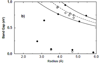
Figure 5. The calculated band gaps are shown by filled symbols. Solid lines are the calculated value and dashed lines are the values predicted by simple TB model. The experimental data are shown by open diamonds. Figure is taken from [31].
They used ![]() 2.53 and γ=.43. The calculated result from this equation does not show good match with experimental data quantitatively. It only gives qualititative better prediction of experimental data than simple TB model.
2.53 and γ=.43. The calculated result from this equation does not show good match with experimental data quantitatively. It only gives qualititative better prediction of experimental data than simple TB model.
Yorikawa et al [31] proposed another equation,
![]() (3)
(3)
Unfortunately, it is also suffered by the same limitation like their previous equation.
Ding et al [19] presented a tight-binding model of SWCNTs with curvature-modified hopping parameter γ0, from which they derived an analytical relation of band gaps to both chirality and diameter by developing a transfer matrix method. Proposed equation of Ding et al is,
![]() (4)
(4)
Where q (=±1) is the mod value.
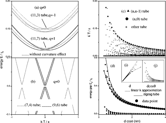
Figure 6. The calculated band structures and energy gaps of chiral tubes (4<m<n<50). Figure is taken from [19].
They found their calculation in agreement with three experimental results obtained from scanning tunneling microscopy and scanning tunneling spectroscopy. One limitation with their equation is, though it includes extra term to reflect curvature effect but it does not include any term to reflect the effect of chirality.
Jorio et al [35] presented the experimental Kataura plot where they plotted experimentally obtained optical transition energies for 200 SWCNTs as a function of tube diameter in a broad range of excitation laser energies (1.26–2.7 eV) and nanotube diameters (0.7–2.3 nm). They proposed following expression to interpret their results:
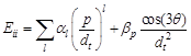 (5)
(5)
In the polynomial expansion on (p/dt), terms up to l = 5 are need for a good description of the observed Eii, where, p = 1, 2, 3, 4 and 5 stands for E11S, E22S, E11M, E33S and E44S, αp is determined by the linear dispersion relation of π-electrons in graphite in tight binding method and βp measures the chiral angle dependence of optical transitions which is different for each Eii subband, increasing for larger i due to the increase of the trigonal warping effect. These two parameters are measured empirically. The plot in Fig. 7 shows deviation of their result from experimental data. The level of deviation goes up to 0.2 eV, as observed from this plot, indicating that deviation of their calculated result from experimental data is not ignorable. One ambiguity in their equation is, it keeps αp and βp undefined, which may vary from case to case.
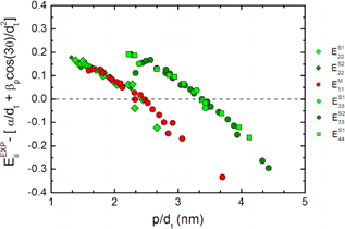
Figure 7. Deviation of the experimentally obtained transition energies from calculated values of [32]. Different symbols stand for different Eii levels and semiconducting mod 1 (S1) and mod 2 (S2). Figure is taken from [35].
Saito et al [20] investigated the effect of trigonal warping on the energy dispersion relations of SWCNTs near the Fermi energy and the chirality dependence of van Hove singularities of the one-dimensional electronic density of states. They derived the width of the transition energy curve in kataura plot in terms of hopping parameter, diameter and chiral angle to reflect the trigonal warping effect on transition energies of metallic and semiconducting SWCNTs.
![]() (6)
(6)
![]() (7)
(7)
This correction term only gives the maximum width of each Eii curve, but it does not give correction to be added with basic TB model equation to reflect trigonal warping effect of mod 1 and mod 2 tubes for any chirality. Moreover, this term is mainly significant for metallic tubes while it’s effect is less on semiconducting tubes because of the small value of sin2(a/6dt). Spataru et al.[24] mentioned that, for semiconducting tubes, this term becomes significant only at higher transitions like E33S.
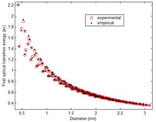
Figure 8. Comparison of experimental E11 with empirically predicted E11 by Jamal et al [42].
Jamal et al[42] proposed a new approach to improve the Tight Binding Model. Based on some arguments, they proposed an empirical formula for nearest-neighbor hopping parameter ![]() in Eqn (1) instead of a constant value so as to calculate first optical transition energy (E11) of semiconducting SWCNTs. The proposed empirical expression for
in Eqn (1) instead of a constant value so as to calculate first optical transition energy (E11) of semiconducting SWCNTs. The proposed empirical expression for ![]() is different for mod 1 and mod 2 type semiconducting SWCNTs as given below:
is different for mod 1 and mod 2 type semiconducting SWCNTs as given below:
![]() to calculate E11 (for mod 1 type):
to calculate E11 (for mod 1 type):
![]() (8)
(8)
![]() to calculate E11 (for mod 2 type):
to calculate E11 (for mod 2 type):
![]() (9)
(9)
They [42] calculated first optical transition energy of 212 semiconducting SWCNTs from Eqn (1) using the above expression of empirical![]() . The agreement between experimental and empirical values was very good over the full diameter range. Average error for E11 over the full diameter range is only 0.0036 eV ( 0.43%) & 0.0033 eV (0.32 %) for mod 1 and mod 2, respectively.
. The agreement between experimental and empirical values was very good over the full diameter range. Average error for E11 over the full diameter range is only 0.0036 eV ( 0.43%) & 0.0033 eV (0.32 %) for mod 1 and mod 2, respectively.
3. First Principle (Ab initio) Based Models
Improvement of computation technology and high speed processors encouraged density function theory based calculation of electronic properties of different materials including SWCNTs. First principles calculations of the electronic band structure in carbon nanotubes first revealed the σ−π rehybridization due to the curvature of the nanotube wall and the failure of zone–folding predictions for very small diameters [7,15,18]. Electron–electron and electron–hole interactions have been included in some of the ab initio - based calculations, predicting a large range of exciton binding energies for different nanotube diameters and dielectric environments.
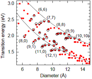
Figure 9. Experimental transition energies, E22s (open symbols) and empirical values calculated by [30] (closed symbols). Only the lower curve is relevant here. Figure is taken from [30].
Reich et al [9], Popov et al [16], Correa et al [7], Gulseren et al [18], Zolyomi et al [15], Bertoni et al [43], Mach on et al [44], Yang et al [45], Liang et al [46] and many other authors performed and reported ab initio calculation of SWCNTs in order to calculate their electronic properties, specially the band structure. Authors used a wide variety of ab initio calculation methods using suitable basis sets, parameters and coding, though in principle they all are same. As it is calculated from atomic level, Ab initio gives results with dependable accuracy, which makes it a scale to measure results from other theoretical models. Consequently, many authors used it to check their theoretical predictions on properties of SWCNTs.
Limitation: Ab initio calculations even within the single - electron picture require a large amount of computational time. Therefore, they are mostly restricted to achiral (armchair and zigzag) tubes or to selected chiral tubes with relatively small unit cells. For chiral nanotubes with unit cells containing more than 100 atoms, this technique is too time consuming to be applied to all (n, m) [40]. Consequently, no complete Kataura plot has been reported so far based on ab initio calculations.
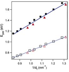
Figure 10. Comparison of the measured band-gap energies (solid symbols) with those predicted by tight-binding theory (open symbols). Solid blue line corresponds to equation proposed by [26]. The dashed blue line is the linear fit to the tight-binding values with γo= 2.9. Figure is taken from [26].
4. Empirical Models
Maultzsch et al [30] presented an empirical relation to determine first optical transition in metallic tubes and thesecond optical transition in semiconducting tubes for more than 50 chiral indices with diameters between 0.6 and 1.5 nm. They started with the basic TB model equation and added a chiral-angle dependent term with it to model the branches of the Kataura plot, which is larger for smaller diameters. The proposed equation for E22 of semiconducting tubes is,
![]() (10)
(10)
Where, γ0= 3.53 eV, γ1= −4.32, and γ2= 8.81 eV and ν is the mod value.
The value of γ0 used by them is quite close to the corresponding parameter in graphite (3.2 eV) and much larger than assumed value for carbon nanotubes in the past (2.5−2.9 eV). Though their equation shows good match with some experimental results but their equation is limited by the short diameter range (0.6 and 1.5 nm) for which they designed it. Its accuracy beyond this range is then doubtful because of its empirical nature.
Dukovic et al [26] ascribed the optical transitions of semiconducting carbon nanotubes to excitons and proposed an empirical relation to calculate band-gap energies of semiconducting SWNTs. They observed that band-gap energies are significantly blue-shifted from values predicted by tight-binding calculations. Proposed empirical relation is,
![]() (11)
(11)
Comparison of their result with Eqn (1) is shown in Fig. 10, where their calculated bandgaps are shown by solid blue line. This plot shows that their result is quantitatively close to experimental values whereas simple TB model calculated values are around 1.6 times lower than experimental values.
But, because of the too simple form of their equation, it becomes nearly a straigt line and cannot give qualitative variation of experimental data, hence cannot reflect many experimental observations. Earlier discussion showed that only the dt term cannot give proper description of optical transitions. In fact, there result can be treated as almost a linear upshipt of tight binding result.
Weisman et al [12] came up with a set of empirical equations to calculate first and second optical transitions in semiconducting SWCNTs with higher accuracy. They fitted Spectrofluorimetric data for a large number of identified single-walled carbon nanotubes to their empirical expressions. They proposed a model-independent prediction of first and second optical transitions as a function of structure for a wide range of semiconducting nanotubes. Their empirical calculation showed very good match with experimental results while differ significantly from simple tight binding model, as expected. They suggested taking their empirical results in preference to conventional model-based predictions because of their higher accuracy.
Weisman et al [12] proposed following empirical equations for mod 1 and mod 2 types semiconducting SWCNTs to calculate their E11 and E22.
E11 of mod 1 type,
![]() (12)
(12)
E11 of mod 2 type,
![]() (13)
(13)
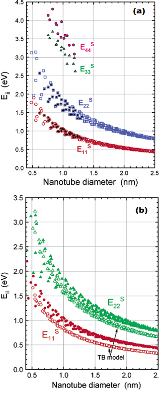
Figure 11. (a) Optical transition energies vs diameter for semiconducting SWCNT. Solid symbols are experimental data; open squares and circles are predictions of E11 and E22, respectively, from the empirical fitting functions. (b) Comparison between model-based and empirical values of optical transition energies for semiconducting SWNT. Open symbols were computed using a simple tight binding (TB) model with γo=2.90 eV, and solid symbols were obtained from the empirically based fitting functions. Figure is taken from [12].
E22 of mod 1 type,
![]() (14)
(14)
E22 of mod 2 type,
![]() (15)
(15)
Figure 11 gives the comparison of their results, as calculated from these equations, with tight binding calculations.
Figure 12 shows Kataura plots from multiple sources for a quick visual comparison between them. A close look on all these approaches reveals that most of them addressed only few SWCNTs of specific chirality and considered only a short range of diameter. For example, approaches of Cao et al [27] and Gulseren et al [18] are limited only to zigzag (n, 0) tubes while that of Correa et al [7] is limited to zigzag and armchair tubes. Jorio et al [35] considered diameter range 0.7–2.3 nm while Dukovic et al [26] considered 0.76 -1.18 nm only. Saito et al [20] offered an expression to reflect trigonal warping effect only.
Proposed empirical relation by Dukovic et al [26] relates first optical transition with diameter only which is not enough to reflect chirality effect. None of these approaches give second optical transition of semiconducting SWCNTs except the one by Maultzsch et al [30] whereas their empirical expression of second optical transition of semiconducting SWCNTs covers diameter range 0.6-1.5 nm only. Also, they did not give first optical transition for semiconducting tubes.
Though the empirical equation proposed by Weisman et al [12] is effective enough to reflect experimental data but it is presented in a complex form that requires some computational efforts due to inclusion of chiral angle, fractional numerical terms and fractional powers. Moreover, they fully ignored basic TB model and formulated a model independent empirical expression to calculate optical transitions by altering the basic form of Eqn (1). So, despite higher accuracy of their empirical expressions, their approach has no relation with improving the TB model calculation. Consequently, their expressions are fully restricted in calculating optical transitionenergies and do not contribute in calculating other electronic properties of SWCNT that could be found by improving existing TB model in a more intelligent way. So, a better model needs to be designed to improve the basic TB model and consequent calculation of optical transition energies.
Hence, these approaches are not comprehensive and they are unable to give accurate prediction of optical transitions in semiconducting SWCNTs of any chirality over a wide diameter range.
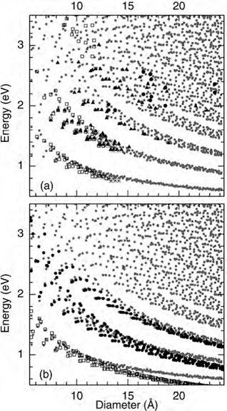
Figure 12. Kataura plots from multiple sources. (a) Experimental data from photoluminescence excitation spectroscopy (open squares, from [12,14] and stars from [48]), resonant Raman scattering (triangles, from [49]), and Rayleigh scattering (full circles, from Reference [13]). (b) Empirical data of Maultzsch et al and Weisman et al (full circles, from [30] and open squares from [12]). Gray dots in (a) and (b) indicate the non-orthogonal tight–binding calculation from Reference [16,50] after a uniform upshift by 0.3 eV. Figure is taken from [40].
Liu et al [47] studied the matter more recently and more extensively than anyone before. They carried a series of optical experiments and measured optical transition energies of numerous semiconducting and metallic SWCNTs. In their work, Liu et al [19] proposed following empirical formula to fit their experimental values of different optical transitions of a number of semiconducting and metallic nanotubes:
![]() (16)
(16)
Here, p is the transition index, k is the magnitude of wave vector in the grapheme Brillouin zone that varies with nanotube chirality (n, m) and transition index p. Magnitude of k is given by p× 2/(3d), where d is the nanotube diameter. Ep(k) is the effective dispersion for transition p, ħ is the reduced Planck constant = 6.582×10⁻¹⁶ ev.s and β=-0.173 ev. nm2. Rest two parameters vF and η have different values for different transition index p.
The empirical formula proposed by Liu et al [47] is superior to other approaches before it due to two reasons. First one is, it fits transition energies of a higher number of SWCNTs than rest other approaches and the second one is, it provides empirical formula up to 10th optical transition energies of SWCNTs whereas rest other approaches are limited in predicting only first two optical transitions. But, one can easily note that the above formula is relatively complex and lot of parameters are involved in calculating any optical transition energy from the above parent equation which increases computational efforts.
Following Kataura plot is a summary of various efforts of calculating optical transition energies which includes theoretical, empirical as well as experimental data from various sources [40].
5. Conclusion
In this work, at first the limitation of the nearest neighbor tight-binding (TB) model in describing accurate electronic properties of single wall carbon nanotube was discussed in brief. Due to those limitations, basic TB model fails to give accurate qualitative and quantitative values of optical transition energies in 1D sub-bands of density of states (DOS) of SWCNT. A review of various approaches to improve the basic TB model to predict different optical transition energies in SWCNTs is presented. Some of them just extended simple π-band model to get better calculation. Some proposed modified or alternative model within or beyond the TB model approach and showed improved calculation using that. Some of them tried to improve TB model Eqn (1) by including extra terms with it which they deduced theoretically or empirically. Some followed first principle calculations for better calculation of the band structure from atomic level. Some took pure empirical approach and proposed model independent empirical equations, without caring Eqn (1).Core points of all those works as well as the advantages and limitations of each of these approaches are highlighted here. This review can help to get an overall idea about various theoretical models and approaches developed or proposed so far to calculate various optical transitions in SWCNTs. Based on this review work one can develop a more improved model that can avoid limitations of all existing models.
References
- V. N. Popov, "Carbon nanotubes: properties and application", Materials Science and EngineeringR, 43, pp. 61–102, 2004.
- T. W. Odom, J. L. Huang, P. Kim, and C. M. Lieber, "Structure and Electronic Properties of Carbon Nanotubes",J. Phys. Chem. B,104,pp.2794-2809, 2000.
- N. Hamada, S. Sawada, and A. Oshiyama, "New one-dimensional conductors: graphitic microtubules," Phys. Rev. Lett., Vol.68,No.10,pp.1579-1581, 1992.
- J. W. Mintmire and C. T. White, "Universal density of states for carbon nanotubes", Phys. Rev. Lett., Vol. 81, No.12, 1998.
- S. Reich and C. Thomsen, "Chirality dependence of the density-of-states singularities in carbon nanotubes", Phys. Rev. B, Vol 62, No. 7, 2000.
- M.S. Dresselhausa, G. Dresselhausc, A. Jorio, A.G. Souza Filho, R. Saito, "Raman spectroscopy on isolated single wall carbon nanotubes", Carbon, 40, pp.2043–2061, 2002.
- J. D. Correa, A. J. R. da Silva, and M. Pacheco, "Tight-binding model for carbon nanotubes from ab initio calculations," J. Phys.: Condens. Matter, Vol.22,No.7, 275503, 2010.
- R. Kundu, "Tight binding parameters for graphene", Modern Physics Letters B, Vol. 25, No. 3, pp.163-173, 2011.
- S. Reich, J. Maultzsch, and C. Thomsen, "Tight-binding description of graphene," Phys. Rev. B, Vol.66,No.3,pp.035412, 2002.
- Y. Lian, Y. Maeda, T. Wakahara, T. Akasaka, S. Kazaoui, N. Minami, N. Choi and H.Tokumoto, "Assignment of the Fine Structure in the Optical Absorption Spectra of Soluble Single-Walled Carbon Nanotubes", J. Phys. Chem. B, 107, 12082-12087, 2003.
- H. Kataura, Y. Kumazawa, Y. Maniwa, I. Umezu, S. Suzuki, Y. Ohtsuka, and Y.Achiba, "Optical properties of single-wall carbon nanotubes," Synthetic Met., Vol.103,pp.2555, 1999.
- R. B. Weisman and S. M. Bachilo, "Dependence of optical transition energies on structure for single-walled carbon nanotubes in aqueous suspension: an empirical kataura plot," Nano Lett., Vol.3,No.9,pp.1235-1238, 2003.
- M. Y Sfeir., T.Beetz, F Wang, L.Huang, X. M. H Huang., M.Huang, J. Hone, S. O’Brien, J. A Misewich, T. F.Heinz, L.Wu, Y.Zhu, L. E. Brus, "Optical Spectroscopy of Individual Single-Walled Carbon Nanotubes of Defined Chiral Structure", Science, Vol. 312, April 2006.
- Bachilo S. M., Strano M. S., Kittrell C.,Hauge R. H., Smalley R. E., Weisman R. B., "Structure-Assigned Optical Spectra of Single-Walled Carbon Nanotubes", Science, Vol 298 No. 5602, pp.2361, 2002.
- V. Zólyomi and J. Kürti, "First-principles calculations for the electronic band structures of small diameter single-wall carbon nanotubes", Phys. Rev. B70, 085403, 2004.
- V. N. Popov,"Curvature effects on the structural, electronic and optical properties of isolated single-walled carbon nanotubes within a symmetry-adapted non-orthogonal tight-binding model", New Journal of Physics, Vol. 6,2004.
- H. Zeng, H. F. Hu, J. W. Wei, Z. Y. Wang, L. Wang, and P. Peng, "Curvature effects on electronic properties of small radius nanotube," Appl. Phys. Lett., Vol.91,No.3,pp.033102, 2007.
- O. Gulseren, T. Yildirim and S. Ciraci,"A systematic ab-initio study of curvature effects in carbon nanotubes", Phys. Rev. B 65, 153405, 2002.
- J W Ding, X H Yan, J X Cao, "Analytical relation of band gaps toboth chirality and diameter of single-wall carbon nanotubes",Phys. Rev. B , Vol. 66, Issue 7, Pages: 2-5, 2002.
- R. Saito, G. Dresselhaus, and M. S. Dresselhaus, "Trigonal warping effect of carbon nanotubes," Phys. Rev. B, Vol.61,No.4,pp.2981-2990, 2000.
- Kane C. L. and Mele E. J., "The Ratio Problem in Single Carbon Nanotube Fluorescence Spectroscopy",Phys. Rev. Lett. 90, 207401, 2003.
- E.J. Mele, C.L. Kane, "Many body effects in carbon nanotube fluorescence spectroscopy", Solid State Communications 135, pp. 527–531, 2005.
- H. Lin, J. Lagoute, V. Repain, C. Chacon, Y. Girard, J.-S. Lauret, F. Ducastelle, A. LoiseauS. Rousset , "Many-body effects in electronic bandgaps of carbon nanotubes measured by scanning tunnelling spectroscopy", Nature Materials 9, 235–238, 2010.
- C. D. Spataru, S. I. Beigi, L. X. Benedict and S. G. Louie,"Excitonic Effects and Optical Spectra of Single-Walled Carbon Nanotubes", AIP Conf. Proc., vol 772, p. 1061-1062, 2004.
- H. Zhao, S. Mazumdar, "Excitons in semiconducting single-walled carbon nanotubes", Synthetic Metals, 155, p.250–253, 2005.
- G. Dukovic, F. Wang, D. Song, M. Y. Sfeir, T. F. Heinz, and L. E. Brus, "Structural dependence of excitonic optical transitions and band-gap energies in carbon nanotubes," Nano Lett., Vol.5,No.11,pp.2314-2318, 2005.
- J. X. Cao, X. H. Yan, J. W. Dingand D. L. Wang, "Band structures of carbon nanotubes: the sp3s*tight-binding model", J. Phys.: Condens. Matter13, L271–L275, 2001.
- A. Hagen and T. Hertel, "Quantitative Analysis of Optical Spectra from Individual Single-Wall Carbon Nanotubes", Nano letters, Vol. 3, No. 3, pp. 383-388, 2003.
- Z. Wang, H. Zhao, and S. Mazumdar, "Quantitative calculations of the excitonic energy spectra of semiconducting single-walled carbon nanotubes within a-electron model", Phys. Rev. B 74, 195406, 2006.
- J. Maultzsch, H. Telg, S. Reich, and C. Thomsen, "Radial breathing mode of single-walled carbon nanotubes Optical transition energies and chiral-index assignment", Phys. Rev. B72, 205438, 2005.
- H. Yorikawa, S. Muramatsu, "Electronic structure characteristic of carbon nanotubules",Z. Phys. B,Condensed Matt., vol. 104, pp. 71–76, 1997.
- A. Jorio, C. Fantini, M. A. Pimenta, R. B. Capaz,Ge. G. Samsonidze, G. Dresselhaus, M. S. Dresselhaus, J. Jiang, N. Kobayashi, A. Grüneis and R. Saito, "Resonance Raman spectroscopy (n,m)-dependent effects in small-diameter single-wall carbon nanotubes", Phys. Rev. B71, 075401, 2005.
- J. Lefebvre, S. Maruyama and P. Finnie, "Photoluminescence: science and applications", Topics in Applied Physics, Vol. 111, pp.287-319, 2008.
- P. K. Valavala, D. Banyai, M. Seel, and R. Pati, "Self-consistent calculations of strain-induced band gap changes in semiconducting (n,0) carbon nanotubes," Phys. Rev. B, Vol.78,No.23,pp.235430, 2008.
- A. Jorio, P. Araujo, S. K. Doorn, S. Maruyama, H. Chacham, and M. A. Pimenta, "The Kataura plot over broad energy and diameter ranges," Phys. Stat. Sol. (b),Vol.243,No.13,pp.3117-3121, 2006.
- H. Yorikawa and S. Muramatsu, "Energy gaps of semiconducting nanotubles," Phys. Rev. B, Vol.52,No.4,pp.2723-2727, 1995.
- H. Yorikawa and S. Muramatsu, "Chirality-dependence of energy gaps of semiconducting nanotubules", Solid State Communications, Vol. 94, Issue 6, Pages 435-437, 1995.
- G. Lanzani, L. Luer, "Carbon Nanotubes: Electronic Structure and Spectroscopy", Comprehensive Nanoscience and Technology,Vol. 1, pp. 23–39, 2011.
- Ge. G. Samsonidze, R. Saito, N. Kobayashi, A. Grüneis,J. Jiang, A. Jorio, S. G. Chou, G. Dresselhaus and M. S. Dresselhaus, "Family behavior of the optical transition energies in single-wall carbon nanotubes of smaller diameters,Appl. Phys. Lett., Vol 85, No. 23, 2004.
- J. Maultzsch, C. Thomsen,"Characterization of Carbon Nanotubes by Optical Spectroscopy,Advanced Micro and Nanosystems",Carbon Nanotube Devices,Vol. 8.,Edited by Christofer Hierold, Verlag GmbH and Co. KGaA, Weinheim, Berlin, Germany, 2008.
- H. Telg, "Raman studies on individual nanotubes and nanotube ensembles –vibrational properties and scattering efficiencies", Ph.d thesis, Physics, Institute für Festkörperphysik,Berlin, 2009.
- G. R. Ahmed Jamal, M. S. Arefinand S. M. Mominuzzaman, "Empirical Prediction of Bandgap in Semiconducting Single-Wall Carbon Nanotubes".Proceeding7th International Conference on Electrical and Computer Engineering (ICECE-2012),pp. 221-224, 20-22 December, 2012, Dhaka, Bangladesh.
- G. Bertoni, L. Calmels, "First-principles calculation of the electronic structure and energy loss near edge spectra of chiral carbon nanotubes", Micron 37, pp.486–491, 2006.
- M. Machón, S. Reich, C. Thomsen, D. S. Portal and P. Ordejón, "Ab initio calculations of the optical properties of 4-Å-diameter single-walled nanotubes", Phys. Rev. B 66, 155410, 2002.
- X. P. Yang, H. M. Weng and J. Dong, "Optical properties of 4 Å single-walled carbon nanotubes inside the zeolite channels studied from first principles calculations", The European Physical Journal B - Condensed Matter and Complex Systems,Vol. 32, No. 3, pp.345-350,2003.
- W. Z. Liang, G. Chen, Z.Li, Z. K. Tang, "Absorption spectra and chirality of single-walled 4 Å carbon nanotubes", Applied Physics Letters, vol. 80 no. 18, pp. 3415-3417, 2002.
- Liu K, Deslippe J, Xiao F, Capaz RB, Hong X, Aloni S, Zettl A, Wang W, Bai X, Louie SG, Wang E, Wang F., "An atlas of carbon nanotube optical transitions", Nat. Nanotech. 7, 325–329, 2012.
- S. Lebedkin, F. Hennrich, T. Skipa, M. M. Kappes, "Near–infrared photoluminescence of single–walled carbon nanotubes prepared by the laser vaporization method",J. Phys. Chem. B, 107, p.1949, 2003.
- P. T. Araujo, S. K Doorn, S. Kilina, S. Tretiak, E. Einarsson, S. Maruyama, H. Chacham, M. A. Pimenta, A. Jorio, "Third and fourth optical transitions in semiconducting carbon nanotubes", Phys. Rev. Lett. , 98,067401, 2007.
- V. N. Popov, L. Henrard, P. Lambin, "Electron–phonon and Electron–photon interactions and resonant Raman scattering from the radial–breathing mode of single-walled carbon nanotubes", Phys. Rev. B , 72,035436, 2005.


