Journal of Nanoscience and Nanoengineering, Vol. 1, No. 2, August 2015 Publish Date: Aug. 3, 2015 Pages: 38-43
Current-Carrying Abilities of Nano-Structured HTS Thin Films
V. I. Matsui, V. S. Flis, V. O. Moskaliuk, A. L. Kasatkin*, N. A. Skoryk, V. L. Svechnikov
Institute of Metal Physics, National Acad. Sci. of Ukraine, Kiev, Ukraine
Abstract
In the present work we study a series of pulse-laser deposited (PLD) high-Tc superconductor (HTS) Y-Ba-Cu-O (YBCO) films with a different defect nano-structure and thickness, namely: (a) pristine YBCO films; (b) YBCO films with implanted Ba-Zr-O (BZO) nano-particles; multilayer YBCO – yttrium oxide (YBCO/YO) films with a sequence (5 layers) of HTS (YBCO) and dielectric phase -yttrium oxide Y-O (YO). All these films were deposited on single crystalline La-Al-O substrates by use of two-beam PLD technique. The critical current density Jc(B,T) dependencies on applied dc magnetic field and temperature for the films under study were obtained from ac susceptibility measurements with a subsequent treatment of experimental results on the base of the Clem-Sanches critical state model. Structural studies of deposited YBCO(BZO) films demonstrate extraction of impurity phase in form of nano-sized particles which are self-organized in columnar c- oriented linear ‘nanorods’ while for the multilayer YBCO/YO films formation of Y-O layers in form of aligned in (ab) - plane extended Y-O nano-particles with high value of aspect ratio (102-103) was observed. The additional defect nanostructure plays the role of strong pinning sites for Abrikosov vortices preventing their motion, thus increasing the critical current value. Moreover, this additional nanostructure, which in YBCO (BZO) films emerges in form of point-like nanoparicles or linear nanorods and in the (YBCO/YO) multylayer films as a high density (ab)-plane stacking faults can improve the current-carrying abilities of these films not only by significant increase of Jc(T,B) absolute value, but also by smoothing of its magnetic field and thickness dependencies. Obtained results distinctly demonstrate that usage of nanotechnological techniques in fabrication of HTS films and coatings allows to improve noticeably their current carrying abilities for needs of modern electric power engineering and electronics.
Keywords
High-Tc Superconductor (HTS), Pulse-Laser Deposition (PLD), Abrikosov Vortex, Pinning, Critical Current
Received: July 8, 2015
Accepted: July 20, 2015
Published online: August 2, 2015
@ 2015 The Authors. Published by American Institute of Science. This Open Access article is under the CC BY-NC license. http://creativecommons.org/licenses/by-nc/4.0/
1. Introduction
Modern electrical engineering demands, conditioned by permanently increasing consumption of electric power, require application of new materials with high current–carrying abilities and low electrical resistance. Just this sort of materials are high–temperature superconductors (HTS) on the base of cuprates RE-Ba-Cu-O (RE – is the rare-earth element: Y, Gd, Nd), produced in a form of thin films and coatings deposited on flexible metallic substrates [1]. Now these HTS tapes are considered as a base for fabrication of lengthy current–carrying conductors for power applications.
Current carrying ability of superconducting material is determined by its critical current density, Jc. For HTS cuprate thin films and coatings produced now by use of modern technologies Jc value at liquid nitrogen temperature (78K) amounts to 106 ¸ 107 А/сm2 [1,2]. Nevertheless, the painstaking work still continues in many laboratories over the world in order to develop the HTS lengthy conductor fabrication technology and to reduce its price, and also to increase the Jc(78К) absolute value and reduce its dependence on magnetic field and thickness of HTS layer [3-7].
Enhancement of flux pinning by optimization of nano-scale defects is fundamental for Jc improvement. High Jc values in HTS films and coatings arise due to strong pinning of magnetic flux (Abrikosov vortices) by nano-sized defects in a crystalline structure of HTS material, which prevent flux motion and emergence of related resistive state of HTS. The Jc value is determined by a pinning force, acting on Abrikosov vortices from these defects, and also by collective interactions within the vortex ensemble [8,9].
Numerous researches of the last decade have demonstrated that different technologies used for deposition of HTS films, such as pulse-laser deposition (PLD) or deposition by use of chemical methods - metal-organic deposition (MOD) can be successfully used for obtaining HTS coatings with high critical current densities Jc (78 K) > 106 A/cm2 on different (including metallic) substrates. The new trend in HTS conductors’ production, which is studied now by numerous research groups, is related to the ‘nanotechnology approach’, namely – implantation of dielectric nano-particles (e.g., BaZrO3, BaSnO3, Y2O3, Y2BaCuO5, etc) in the interior of HTS layer. These implanted nano-particles form additional strong pinning centres for Abrikosov vortices – point-like and also extended linear ones (so called ‘nanorods’, which can arise due to self-assembling of nano-particles) and do not deteriorate the texture of a superconductor [1,2,10,13].
There is also another approach for obtaining HTS layers with enhanced Jc values, which is based on deposition of multilayer HTS/insulator structures [5,15]. This approach is supported by the well-known result, obtained for HTS thin films and coatings, namely: decrease of the Jc value with increase of the layer thickness. So, separation of the total HTS layer thickness into few HTS sub-layers separated by dielectric phase thin layers could lead to enhance of the total critical current of the HTS coating [14-17].
Despite the achieved progress in fabrication and study of HTS conductors with high current-carrying capability, the distinct relation between the critical current density (and its dependence on magnetic field, temperature and HTS layer thickness - Jc(B,T,d)) and HTS material nano-structure features has not been established yet. There are some empirical relations in this field, nevertheless there is no clear understanding how to get further increase of Jc values and also to diminish its dependence on magnetic field and HTS layer thickness. In particular, there are open questions which concern maximal possible values of Jc and optimization of the defect nano-structure allowing to obtain these maximal Jc values.
2. Experimental
The superconducting films were manufactured by pulse laser deposition on to single crystal (100) LaAlO3 substrates by use of dual-beam PLD technique. (see Fig.1). Two identical optical lines of Q-modulated Nd: YAG lasers (wavelength 1064 nm) and optical amplifiers were used. The pulse energy Wp reached 240mJ at pulse duration τp =7,5ns and fr = 25 Hz repetition rate. Synchronism of two laser pulses coming on the target was ∆τ ≤ 300ps. Pure stoichiometric YBa2Cu3O7-x targets as well as doped with 3.0 (mass%) of BaZrO3 were used. The targets YBa2Cu3O7-x, Y2O3 and YBCO+BZO 3%, were made by powder sintering of corresponding compounds prepared by solid state synthesis. All reference films were first deposited on single crystal (100) LaAlO3 substrates.
The reference, pure YBa2Cu3O7-δ, BZO-doped YBCO, Y2O3 layers were grown by PLD ablation with the laser pulse power density Pft=(Wp/τp) on the target varied in the range 0,867∙109W/cm2 ¸ 12.2∙109W/cm2. The temperature of cilindric targets consisted 240ºC - 260ºC. The substrate temperature Ts was ranged from 740ºC to 800ºC, the deviation of target temperature did not exceed 0,35ºC during 10 min of deposition, while the partial oxygen pressure pQ2 within camera was supported at the level 34Pa. The distance between the targets and substrate Lts was equal 52mm. BZO-doped (3 wt%) YBCO films were deposited in PLD chamber following the same procedure as that for the reference samples. Deposition of YBCO/Y2O3 multilayer films was performed by use of cylindrical targets for both compounds, which were placed closely on the axis of rotation mechanism. Thus it was possible to deposit the multilayer film with an adjusted structure by changing the ablation time for each of two targets .The deposition rate strongly depends on Pft, Ts, pQ2, Lts and for YBCO film was about 28 nm/min -25nm/min, while for BZO-doped YBCO deposition rate was about 30 nm/min -26nm/min, and for Y2O3 layers it was about 16nm/min -14nm/min.
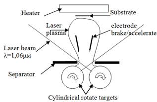
Figure 1. Schematic presentation of the dual-beam pulse laser deposition technique.
In the present work we study a series of pulse laser deposited (PLD) YBa2Cu3O7-d (YBCO) films with a different defect nano-structure and thickness, namely: (a) pristine YBCO films; (b) YBCO films with implanted BaZrO3 (BZO) nano-particles; multilayer YBCO/Y2O3 films with a sequence (5 layers) of HTS (YBCO) and dielectric phase (Y2O3). Characteristics of the deposited films under study are presented in Table 1.
Table 1. Characteristics of the deposited films under study.
| Number of the film | Substrate [size film mm x mm] | Thickness layers (nm) | Composition and structure films | Тс, K | ΔT,K | Jc, MA/cm2 |
| pp-91/1 | LaAlO3 [10x10] | 240 | YBCO | 88,8 | 1,21 | |
| рр-78/2 | LaAlO3 [10x10] | 360 | YBCO | 90,78 | 2,9 | |
| рр-76/3 | LaAlO3 [10x10] | 600 | YBCO | 91,07 | 3,88 | |
| pp-84/4 | LaAlO3 [10x10] | 240 | YBCO+BZO 3% | 90,88 | 2,43 | |
| рр-82/5 | LaAlO3 [10x5] | 360 | YBCO+BZO 3% | 91,43 | 2,03 | |
| рр-92/5 | LaAlO3 [5x5] | 600 | YBCO+BZO 3% | 89,05 | 1,35 | |
| рр-86/5 | LaAlO3 [5x5] | 300nm+40nm | YBCO (5 layers х60 nm) +Y2O3 (4 layers х 10 nm) | 90,74 | 1,04 | |
| рр-90/8 | LaAlO3 [5x5] | 260nm+80nm | YBCO (5 layers х 52 nm) +Y2O3 (4 layers х 20 nm) | 92,34 | 2,47 |
Microstructure and surface morphology of films were investigated by use of transmission electron microscopy (TEM, JEOL 3000F), scanning electron microscopy (SEM, FEI Inspect F) and atomic force microscopy (AFM). Detailed description of such kind structural studies are presented in the authors works [18, 19]. Critical current measurements were performed by use of the dynamic magnetic susceptibility method in the frequency range 200-1000 Hz. This method, accompanied by a theoretical treatment, based on the critical state model for magnetic flux penetration inside the superconducting film, allows to determine the critical current density of the film from measurements of the imaginary part of complex ac magnetic susceptibility dependence c²(Hac) on ac magnetic field amplitude Hac. The magnetic field dependencies Jc(B) were obtained at 77 K in the field range of 0¸1 T for the case when magnetic field B was oriented parallel to the c-axis of the film.
3. Results and Discussion
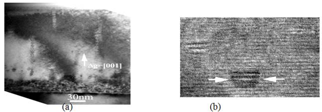
Figure 2. TEM images of YBCO(BZO) deposited films cross sections: (a) lattice of nanorods parallel to the c axis of the crystalline matrix; (b) stack of BZO nanoparticles which forms ‘nanopancake’.
The TEM images of cross sections of YBCO(BZO) films (Fig. 2(a)) demonstrate extraction of impurity phase in form of nano-sized particles which are self-organized in columnar c- oriented linear ‘nanorods’. A typical diameter value for these nanorods is 5¸20 nm. As one can see from Fig.2, the crystal structure of nanorods may be adjusted with the crystal structure of matrix or may be tilted by 3–4° relatively to its c- axis. As a rule, nanorods are generated in the damaged layer of the film close to the substrate and terminate at the free surface, but sometimes they can start and end inside the film, as it is shown in Fig. 2(a) (particularly in the regions where (001) planes are significantly deformed). The nanorods can also noticeably deviate from the normal direction to the films substrate.
As can be seen from the Fig. 2 (b), besides nanorods, there is also another type of nano-sized inclusions in doped YBCO(BZO) films. These are planar particles with a small diameter (less than 3 nm), called ‘nanopancakes’ [18,19]. The distances between the nanopancakes are about 20–40 nm, and this is commensurable with the distances between the low-angle boundaries which separate single-crystal domains (grains) in the film. Thus, the implantation of nano-sized dielectric particles in the matrix of HTS film leads to emergence of an additional linear and point-like pinning centres for Abrikosov vortices (‘nanorods’ and ‘nanopancakes’, respectively). Besides, these extra nano-sized dielectric particles can serve not only as an effective vortex pinning centers, but they can also disrupt the YBCO matrix around them and produce additional dislocations in the YBCO films interior (see Fig. 3). These dislocations also serve as a strong pinning centre for Abrikosov vortices.
For multilayer YBCO/Y2O3 films structural studies were carried out by use of SEM technique. Specific features which concern distribution of Y2O3 in YBCO/Y2O3 multilayer films are presented in Fig.4. As one can see, the Y2O3 compound tends to grow within the (ab) - plane aligned layers in form of extended particles with a high aspect ratio value (102-103). For low thickness of Y2O3 layer it forms the discontinuous, fern-like structure. When thickness of the Y2O3 layer exceeds 20nm, then conditions for formation of continuous YBCO/Y2O3 films with separated superconducting YBCO and dielectric Y2O3 layers become favourable.
We have studied transport properties of YBCO(BZO) and YBCO/Y2O3 multilayer films in applied perpendicular magnetic field and compared these results with similar ones obtained for pristine YBCO films.
Magnetic field dependencies of the critical current density Jc(В, 78K) of the films under study, determined by dynamic magnetic susceptibility method [19], are presented in Fig.5. One can see from Fig.5 and Table 1 that Jc(0, T=77 K) value for pristine YBCO films decreases rather quickly with increase of the films thickness, while addition of BZO nano-particles in the films interior for YBCO(3%BZO) makes this decrease significantly slower. Also, the Jc(0, T=77 K) value increases from 0,81 MA/cm2 for pure YBCO film with a thickness d = 600 nm up to 1.67 MA/cm2 for YBCO(3%BZO) film with the same thickness. In YBCO/Y2O3 multilayer films Jc(0, T=77 K) value reaches 2.69 MA/cm2 for the thickness value d = 360 nm.
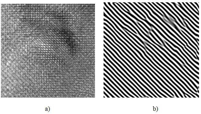
Figure 3. HREM images of YBCO(3%BZO) films: (a) separate BZO nanoparticle within the YBCO film matrix; (b) – formation of additional dislocations around BZO nanoparticle.
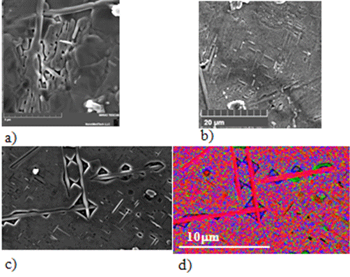
Figure 4. SEM images of Y2O3 layer deposited on YBa2Cu3O7-δ layer of multilayer film: (a,b) - thickness of the Y2O3 layer -35nm;(c,d)-10nm. (d)- colour map of element distribution over the layer: green- Cu, red- Y, blue- Ba.
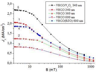
Figure 5. Magnetic field dependencies of the critical current density for YBCO, YBCO(BZO) and YBCO/Y2O3 multilayer films with different thickness.
Enhancement of Jc value in YBCO(BZO) films comparatively to that in pristine YBCO films is due to additional pinning of Abrikosov vortices by BZO nanorods splayed around the c-axis as well as randomly distributed small planar nano-particles - ‘nanopancakes’ [19]. For YBCO/Y2O3 multilayer films local irregularities of Y2O3 layers aligned in (ab)- plane can be considered as high density (ab)-plane stacking faults and also act as pinning centers for vortices. In both cases additional pinning sites improve Jc not only by its value, but also by its magnetic field dependencies, making Jc(B) dependencies more gentle. It was supposed that the addition of BZO nano-particles in YBCO material is detrimental with regard to the critical temperature Tc value [20,21]. This may proceed due to local strain fields caused by the lattice mismatch between YBCO and BZO phases and the consequent local oxygen deficiency, which probably occurs around BZO phase inclusions. It worth to notice that we have no observed an essential decrease of Tc for YBCO(3%BZO) samples as well as for YBCO/Y2O3 multilayer films. The most characteristic features of the measured Jc(В) dependencies are: (a) - existence of the plateau at small fields (В < 10 ¸50 mT), resulting from individual pinning of Abrikosov vortices on structural defects, and (b) - subsequent power-like decrease of Jc(В) value: Jc(В) µ В-a (a > 0) at higher fields. The latter is related to collective effects in the vortex ensemble at high magnetic fields [8,9]. The power exponent α was calculated from the log–log plot of Jc(B) dependence. The exponent value of pure YBCO thin is found to be ~0,5 which is commonly observed for PLD YBCO films [7]. The exponent values for YBCO(3%BZO) samples are found to be ~0.38, and 0,43for YBCO/Y2O3 multilayer films with Y2O3 layer thickness ~10 nm. Such a decrease of a value suggests a lesser field dependence of Jc(B) in YBCO(BZO) and YBCO/Y2O3 films.
4. Conclusion
It was shown that usage of nanotechnological approaches in HTS thin films formation, such as addition of the impurity phase nanoparticles (BZO) or deposition of multilayer films HTS/insulator (YBCO/Y2O3), can significantly improve the current-carrying capabilities of HTS conductors and make them more attractive for power applications. The additional defect nanostructure, which arises due to these deposition technology improvements, plays the role of strong pinning sites for Abrikosov vortices, preventing their motion, thus increasing the critical current value. Moreover, this additional nanostructure, which in YBCO(BZO) films emerges in form of point-like nanoparicles or linear nanorods and in the (YBCO/Y2O3)multylayer films as high density ab-plane stacking faults can significantly improve Jc not only by its value, but also by its magnetic field and thickness dependencies.
Acknowledgements
This work was supported by the National Academy of Sciences and National Science Council of Ukraine through the program "Nanotechnologies and nanomaterials".
List of Notations
HTS – high-temperature superconductor
PLD – pulse-laser deposition
YBCO – YBa2Cu3O7-x compound
BZO – BaZrO3 compound
T – temperature in (K)
B – magnetic field in (T)
Jc– critical current density in (A/cm2)
References
- S. R. Foltyn, L. Civale, J. L. MacManus-Driscoll, Q. X. Jia, B. Maiorov, H. Wang , M. Maley,Nature Mater. 6, 631 (2007).
- B. Maiorov, S. A. Baily, H. Zhou, O. Ugurlu, J. A. Kennison, P. C. Dowden, T. G. Holesinger, S. R. Foltyn, L. Civale , Nature Mater. 8, 398 (2009).
- M. Miura, B. Maiorov, S. A. Baily, N. Haberkorn, J. O. Willis, K. Marken, T. Izumi, Y. Shiohara, L. Civale , Phys. Rev.B 83, 184519 (2011).
- V. Braccini, A. Xu, J. Jaroszynski, Y. Xin, D. C. Larbalestier, Y. Chen, G. Carota, J. Dackow, I. Kesgin, Y. Yao, A. Guevar, T. Shi, V. Selvamanickam, Supercond. Sci. Technol. 24, 035001 (2011).
- A Kiessling, J Hänisch, T Thersleff, E Reich, M Weigand, R Hühne, M Sparing, B Holzapfel, J H Durrell, L Schultz, Supercond. Sci. Technol. 24, 055018 (2011).
- S. I. Kim, F. Kametani, Z. Chen, A. Gurevich, D. C. Larbalestier, Appl. Phys. Lett. 90, 252502 (2007).
- H. Matsui, H. Ogiso, H. Yamasaki, T. Kumagai, M. Sohma, I. Yamaguchi, T. Manabe, Appl. Phys. Lett. 101, 232601 (2012).
- E. H. Brandt, Rep. Progr. Phys. 58, 1465 (1995).
- G. M. Blatter, M. V. Feigel'man, V. B. Geshkenbein, A. I. Larkin, V. M. Vinokur, Rev. Mod. Phys. 66, 1125 (1994).
- P. Mele, K. Matsumoto, A. Ichinose, M. Mukaida, Y. Yoshida, S. Horiie, R. Kita,Physica C, 469, 1380 (2009).
- D. H. Tran, W. B. K. Putri, B. Kang, N. H. Lee and W. N. Kang, J. Appl. Phys. 115, 163901 (2014).
- H. Zhou, B. Maiorov, S. A. Baily, P. C. Dowden, J .A. Kennison, L. Stan, T.G. Holesinger, Q. X. Jia, S. R. Foltynand, L. Civale, Supercond. Sci. Technol. 22 , 085013 (2009).
- A. Xu, L. Delgado, N. Khatri, Y. Liu, V. Selvamanickam, D. Abraimov, J. Jaroszynski, F. Kametani, D. C.Larbalestier, APL Materials 2, 046111 (2014) .
- S. Kang, K.J. Leonard, P. M. Martin, J. Li , A. Goyal, Supercond. Sci. Technol. 20, 11 (2007).
- H. Huhtinen, K. Schlesier, P. Paturi, Supercond. Sci. Technol.22, 075019 (2009).
- V. F. Solovyov, H. J. Wiesmann, L. Wu, Q. Li, L. D. Cooley, M. Suenaga, B. Maiorov, L. Civale, Supercond. Sci.Technol.20, L20 (2007).
- T. G. Holesinger, M. D. Feldmann, B. Maiorov, L. Civale, J. A. Kennison, Y. J. Coulter, P. D. Dowden, J. F. Baca, P. H. Tobash, D. Bauer, K. R. Marken, Materials 4, 2042, (2011).
- V. L. Svechnikov, V. S. Flis, A. A. Kalenyuk, A. L. Kasatkin, A. I. Rebikov, V. O. Moskaliuk, C. G. Tretiatchenko, V. M. Pan, J. Phys.: Conf. Ser. 234, 012041 (2010).
- V. S. Flis, A. A. Kalenyuk, A. L. Kasatkin, V. O. Moskaliuk, A. I. Rebikov, V. L. Svechnikov, C. G. Tret’yachenko, V. M. Pan, Low Temp. Phys.36, 59 (2010).
- T. Aytug, M. Paranthaman, E. D. Specht, Y. Zhang, K. Kim, Y. L. Zuev, C. Cantoni, A. Goyal, D. K. Christen, V. A.Maroni, Y. Chen, V. Selvamanickam, Supercond. Sci. Technol. 23, 014005 (2010).
- S. H. Wee, Y. L. Zuev, C. Cantoni, and A. Goyal, Sci. Rep. 3, 2310 (2013).


