
Journal of Nanoscience and Nanoengineering, Vol. 1, No. 2, August 2015 Publish Date: Aug. 17, 2015 Pages: 96-106
Limitations of Tight Binding Model in Describing Electronic Properties of Single Wall Carbon Nanotubes
G. R. Ahmed Jamal1, *, S. M. Mominuzzaman2
1Department of Electrical and Electronic Engineering, University of Asia Pacific, Dhaka, Bangladesh
2Department of Electrical and Electronic Engineering, Bangaldesh University of Engineering and Technology, Dhaka, Bangladesh
Abstract
Carbon nanotubes are one of the most intensively studied materials in recent decades. The tight-binding (TB) model of π-bands of graphene using the zone-folding approximation has been widely used for modeling electronic band structure of single-wall carbon nanotube (SWCNT) due to its simplicity and low computational cost. However, thorough investigation and detailed comparison of the result from this theoretical model with various recent optical spectroscopic experiments reveals that TB models fails quantitatively and in some cases qualitatively to predict different optical transition energies in SWCNTs. Many authors discussed this issue through theoretical and experimental results and showed the limitation of TB model in describing SWCNTs. The purpose of this work is to discuss various limitations of TB model of SWCNTs along with main theoretical factors that limit this model. This work will presents a summary and review of some important previous research works by different authors highlighting the limitations of Tight-binding (TB) model, especially its nearest-neighbor approximation. This work will also focus on findings by various researchers regarding the main factors that cause the tight binding model given electronic band structure and corresponding transition energies to deviate from experimental results. This review work concludes that the TB model greatly fails in describing SWCNTs.
Keywords
Carbon Nanotube, SWCNT, Tight Binding Model, Optical Transition Energy, Chiral Index
Received: July 2, 2015
Accepted: August 3, 2015
Published online: August 17, 2015
@ 2015 The Authors. Published by American Institute of Science. This Open Access article is under the CC BY-NC license. http://creativecommons.org/licenses/by-nc/4.0/
1. Introduction
Since the discovery of Carbon Nanotubes (CNT) by Sumio Iijima [1,2] in 1991, they become one of the most intensively studied materials and are gaining more and more attention to researchers in every year. For their unique one-dimensional nanostructure and extraordinary electronic, optical, mechanical and chemical properties, CNTs are considered as an ideal building block for next-generation molecular electronic and optoelectronic devices and circuits [3,4].
Electronic and optical properties of single-wall carbon nanotubes (SWCNT) are directly associated with their geometrical structures [5,6] which are uniquely specified by a pair of chiral index (n, m). A SWCNT (n, m) will be metallic if its n-m = 3k (k is integer), i.e. mod (n-m, 3) = 0 and it will be semiconducting if its n-m ≠ 3k, i.e. mod(n-m, 3) = 1 or 2 [7]. This relation gives two types of semiconducting SWCNTs, mod 1 type and mod 2 types. Also, this relation indicates that theoretically two third of the total SWCNTs are semiconducting and one third are metallic.
The one-dimensionality of the nanotubes gives rise to 1D sub-bands instead of one wide electronic energy band in nanotube density of states (DOS), as shown in Fig 1. Each SWCNT (n, m) has a unique set of interband transition energies Eii denoting the energy differences between the i-th conduction and valence bands and optical transitions can only occur between these mirror sub-bands [5,6,8,10]. These singularities are unique feature of nanotubes and also primarily responsible for many distinguished electronic and optical properties of SWCNTs.
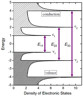
Figure 1. Schematic density of states diagram for a semiconducting single-walled carbon nanotube, in a simple band theory model. Allowed optical transitions are illustrated as vertical arrows.
Many applications of semiconducting SWCNT require prior information of these optical transition energies (specially, the bandgap energy). Hence, accurate calculation of their optical transition energies from a theoretical model is a necessity. The tight-binding (TB) model of π-bands of graphene using the zone-folding approximation has been widely used for modeling electronic band structure of single-wall carbon nanotube (SWCNT) due to its simplicity, low computational cost, and qualitative agreement with experimental results [11-13]. TB model with the nearest-neighbor approximation provides following simple expression to calculate optical transitions of a semiconducting nanotubes [5,6,14]:
![]() (1)
(1)
Where, ![]() is the nearest-neighbor hopping parameter,
is the nearest-neighbor hopping parameter, ![]() Å is carbon-carbon bond length,
Å is carbon-carbon bond length, ![]() is nanotube diameter in nm, given by
is nanotube diameter in nm, given by ![]() and j is an integer. Eii corresponds to the first, second, third, fourth…… interband transitions (E11S, E22S, E33S, E44S….) of semiconducting SWCNT when j = 1, 2, 4, 5… respectively, and to the first and second interband transition (E11M, E22M ) of metallic SWCNT when j = 3 and 6, respectively. This inverse proportional trend of transition energies with SWCNT diameter, given by Eqn. (1), is also observed from the Kataura plot [15,16] and from other optical spectroscopic experiments [10,17].
and j is an integer. Eii corresponds to the first, second, third, fourth…… interband transitions (E11S, E22S, E33S, E44S….) of semiconducting SWCNT when j = 1, 2, 4, 5… respectively, and to the first and second interband transition (E11M, E22M ) of metallic SWCNT when j = 3 and 6, respectively. This inverse proportional trend of transition energies with SWCNT diameter, given by Eqn. (1), is also observed from the Kataura plot [15,16] and from other optical spectroscopic experiments [10,17].
Here, the first optical transition (E11) is the bandgap of semiconducting SWCNTs and the second optical transition (E22) facilitates various optical spectroscopic experiments, as it falls within visible energy range. Also, for photo absorption, first two optical transitions are mainly considered. Hence, E11 and E22 of semiconducting SWCNTs are more significant than other transitions and are of more interest [18].
The qualitative agreement of Eqn (1) with experimental results is good [11], but it fails to predict optical transition energies with quantitative accuracy to the limit that it underestimates and overestimates first and second optical transition energies of semiconducting SWCNTs (E11S, E22S) around 25% even with the best choice of ![]() as a fitting constant parameter [16]. Its quantitative failure is more prominent for lower diameter tubes [19,21]. Equation (1) also fails to reflect relative difference between mod 1 and mod 2 type semiconducting SWCNTs for odd transitions (like, E11) and even transitions (like, E22) with comparable diameter [17] and gives incorrect ratio of first two optical transitions [18], as observed from various optical spectroscopic experiments.
as a fitting constant parameter [16]. Its quantitative failure is more prominent for lower diameter tubes [19,21]. Equation (1) also fails to reflect relative difference between mod 1 and mod 2 type semiconducting SWCNTs for odd transitions (like, E11) and even transitions (like, E22) with comparable diameter [17] and gives incorrect ratio of first two optical transitions [18], as observed from various optical spectroscopic experiments.
The objective of this work is to present a review of some important previous research works to highlight the limitation of Tight-binding (TB) model, especially its nearest-neighbor approximation. This work also present a review of findings by various researchers regarding the main factors that cause the tight binding model given electronic band structure and corresponding transition energies to deviate from experimental results.
2. Limitations of Tight Binding Model
Reich et al [13] studied the band structure of isolated and bundled single wall carbon nanotubes on the basis of ab initio calculations and discussed the limits of the graphene π-band TB model in describing the SWCNT bands. They [13] also made the TB parameterization for the graphene taking into account the interaction to third neighbors and fitting the graphene band structure to the calculated TB parameters. They compared their ab-initio result with nearest-neighbor and third nearest neighbor TB model calculation as shown in Fig. 2. Correa et al [11] presented a similar comparison of TB model from ab initio calculations, but with a reduced set of parameters.
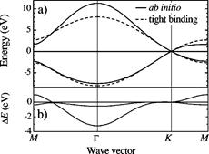
Figure 2. Ab initio and nearest-neighbor tight-binding dispersions of graphene. (a) The converged ab initio calculation is shown by the full lines. The dashed lines represent the tight-binding dispersion with so= 0 and γo= 2.7 eV. (b) Difference ΔE between the ab initio and tight-binding band structures. Figure is taken from [13].
Tight binding model also fails to account some specific tendencies of transition energies observed from some optical spectroscopic experiments. Sfeir et al [17] observed from their Rayleigh scattering experiment that the mod 1 type semiconducting SWCNT have smaller transition energies than mod 2 type for odd transitions (E11S, E33S,….) whereas, mod 2 type semiconducting SWCNT have smaller transition energies than mod 1 type for even transitions (E22S, E44S,….) with comparable diameters. This observation is not reflected by Eqn (1) as it gives comparable values of transition energies for comparable diameters with any constant![]() , irrespective of mod type.
, irrespective of mod type.
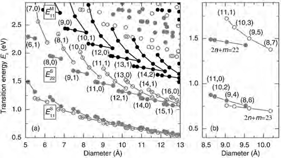
Figure 3. A practical Kataura plot. The gray symbols indicate mod 1 (closed circles) and mod 2 (open circles) semiconducting tubes. The lines connect 2n + m families. Right most box shows zoom into the E11S and E22S region of two family branches; Within a branch, neighboring tubes from left to right are given by ( n−1, m + 2). Figure is taken from [23].
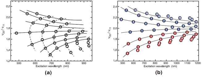
Figure 4. Comparison of flourescence spectroscopy result with TB calculation. (a) Measured ratios of excitation to emission frequencies by Bachilo et al (b) Computed ratio from an extended TB model for mod 1 type (blue) and mod 2 type (red). Soild lines connect families with equal n – m values and dotted line connects 2n+m families. It can be observed that, for large diameters, lines converge to near 1.75 in (a) and near 2 in (b). Figure is taken from [18].
In addition to this, experimental observation showed a systematic pattern of optical transition energies in kataura plot (Eii vs dt plot), depending on their mod (n-m, 3) = 0, 1 or 2. As shown in Fig. 3, SWCNTs having same (2n+m) values form branches in kataura plot, showing "family behavior" of transition energies [22]. SWCNTs associated with each branch are termed as member of that (2n+m) family [23]. The observed family behavior causes deviation of Kataura plot from TB model predicted simple Eii α 1/dt relation. Though zone folding provides an explanation of this observation but it is not reflected through Eqn (1) as it gives comparable values of transition energies for comparable diameters with any constant![]() , irrespective of their mod type.
, irrespective of their mod type.
Okada et al [24] also reported the relative difference between optical transition energies of mod 1 and mod 2 types. They studied the electronic structure of all the semiconducting SWCNTs having diameters between 0.75 nm and 1.55 nm. The Kataura plot calculated by them differed from the corresponding plot obtained from zone-folding model.
Equation (1) also fails to account experimentally observed ratio of first two optical trasnsition energies of semiconducting SWCNTs (E22S/E11S). Simple linearized tight-binding model predicted this ratio to be 2 from Eqn (1). Extended TB model
later predicted that this ratio will be lesser than 2 at small diameters but will approach 2 asymptotically for large diameters [25]. In practice, experimentally observed ratio was found to oscillate below and above 2 (down to 1.17 and up to 2.6) for different chiralities and converge to only around 1.8 for large diameters [25-29]. This problem is often referred as ‘ratio problem’ in literatures [25]. Neither the simple TB model nor the extended TB model could account this observation fully.
In 2002, Bachilo et al [18] and O’ Connel et al [30] independently performed two very important flourescence spectroscopy experiments and observed band gap luminescence from SWCNTs for the first time. Bachilo et al [18] observed that absorption (E22) and emission (E11) energies from SWCNTs differ from theoretical predictions of tight binding calculations. Their measured optical transition frequencies (υii) significantly deviate from simple diameter dependence more strongly than expected. For example, they found υ22 value of the (9,2) tube is 26% higher (by 3700 cm-1 or 0.46 eV) than that of (9,1), even though its diameter is only 6% larger. In addition, as tube diameter increases, they found the υ22/ υ11 (or, E22/E11) ratio apparently approaches a value around 1.75, smaller than tight binding prediction, i.e. the ‘ratio problem’. Their excitation vs emission frequency plot showed a blue shift of these frequencies though they did not highlight this observation in their report.
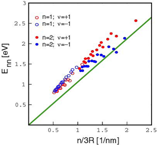
Figure 5. Observed ‘blue shift’ of optical transition energies measured from fluorescence spectroscopy, for mod 1 type (ν =+1) and mod 2 type (ν = -1) semiconducting SWCNTs. The solid line gives the prediction of linearized TB model theory. Figure is taken from [26].
Kane et al [25] and Mele et al [26] reported ‘blue shift’ of transition energies which is also not reflected through Eqn (1) They observed this problem after scrutinizing flourescence spectroscopy results reported by Bachilo et al [18] and O’ Connel et al [30]. They plotted observed optical energies of SWCNTs measured in fluorescence spectroscopy as a function of n/3R and showed that E11 and E22 deviate from simple linearized tight binding model and are blue shifted by a nonlinear 1/R scaling. They termed this observation as ‘blue shift problem’ [17,26,31].
Zhao et al [29] discussed both the ‘ratio problem’ and the ‘blue shift problem’. As per their analysis, the ratio problem is a simple consequence of nearly equal blueshifts of the two lowest optical absorptions (E11 and E22) from TB frequencies.
3. Factors that Limit the Tight Binding Model in Describing SWCNTs
These disagreements of Eqn (1) are attributed to many factors. One major factor is nanotube ‘curvature effect’ induced band structure deviation from simple π-orbital graphene picture [19-21,32]. Other factors are ‘chirality effect’ [33], ‘trigonal warping effect’ [17,19,34] and many body effect (electron-electron interaction) comprising self-energy and exitonic effect [25-29,31].
These factors and their effects are discussed below:
3.1. Curvature Effect
The first factor is nanotube ‘curvature effect’ [11,19,21,32,33]. It causes deviations in the electronic properties of nanotubes derived from the simple π-orbital graphene picture due to nanotube curvature.
A weakness of the zonefolding approximation is, it totally neglected the curvature of the tube walls [35]. In the zone-folding derivation of the electronic band structure of SWCNTs, nanotubes were essentially treated as graphene sheets with a periodic boundary condition. In doing so, it is assumed that π-orbitals are still orthogonal to σ-orbitals in the graphene plane so that we can treat π orbitals independently as in the graphene case [36]. As SWCNTs are not just stripes of graphene but small cylinders [37], this assumption, however, is not valid due to the tube curvature [36], which forces the naturally flat sp2 bonds to bend [35].
There are three important consequences of this curvature on nanotube structure:
1) Curvature causes π and σ states to mix, as the planar symmetry is broken. This leads to hybridization between σ and π orbitals and charge self-consistency become important. The degree of hybridization becomes larger as the diameter of a SWCNT gets smaller [36-38].
2) Formation of an angle for the pz orbitals located on bonds not strictly parallel to the axis, i.e. de-localization of π bond orbitals. This results non-identiacal hopping terms (γo) between a carbon atom and its three nearest neighbors [37,38].
3) C-C bonds perpendicular and parallel to the axis are slightly different and therefore the graphene basis vectors a1 and a2 are not of exactly equal length anymore [37].
The σ–π hybridization effect has been considered and calculated in the literature [19-21,32,33]. The main result is that nanotubes satisfying |n−m| = 3I (I=0, 1, 2….) develop a small curvature-induced bandgap, and hence become quasi-metallic or small gap semiconductor [38]. Armchair nanotubes are an exception because of their special symmetry, and only they remain truly metallic for all diameters [38]. On the other hand, some lowest diameter tubes with |n−m| ≠ 3I are found to be metallic due to high curvature in them. In zigzag and chiral metallic nanotubes, the Fermi point is no longer included in the allowed states and a small bandgap opens at the Fermi level. This band gap is called secondary band gap and it varies as 1/dt2 (both theoretically predicted and experimentally observed). The secondary band gap is usually so small for quasi-metallic zigzag nanotubes that all n - m = 3I (I=0,1,2,. . .) nanotubes can be considered as metallic at room temperature [37]. For example, while a semiconducting nanotube with a diameter of 1 nm has a bandgap of 0.7 eV, a quasi-metallic nanotube with a comparable diameter has a bandgap of only 40 meV [38]. Since curvature becomes larger with decrease in nanotube diameter, deviations from the simple π-orbital graphene picture become more important in small diameter nanotubes. Higher degree of σ–π hybridization occurs in small diameter nanotubes which significantly alters their electronic properties [37]. It has been found that, while tight-binding calculations predict small diameter (4, 0) and (5, 0) zigzag nanotubes to be semiconducting with bandgaps exceeding 1 eV, ab initio calculation shows that they are metallic. Similarly, while tightbinding calculations predict that the (6, 0) zigzag nanotube is quasi- metallic with a bandgap of approximately 200 meV, ab initio calculations indicate that they are truly metallic [38,39].
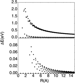
Figure 6. Energy Gaps calculated for all tubes with diameter less than 3 nm. The tubes fall into three families: those with primary gaps which scale as 1/R (top panel, top curve), those with zero primary gap but nonzero curvature induced gaps which scale as 1/R2 (lower curve top panel, and shown in the expanded scale in the lower panel), and armchair tubes with zero primary gap and zero curvature induced gap. Figure is taken from [39].
Popov et al [20] studied the effects of nanotube curvature on electronic and optical properties of isolated single-walled carbon nanotubes within a symmetry-adapted non-orthogonal tight-binding model using 2s and 2p electrons of carbon. The calculated transition energies from this model show agreement with ab-initio result but deviate widely from π-band tight-binding model calculation, especially for small radius tubes.
Gulseren et al [32] investigated curvature effects on electronic structure of zigzag nanotubes from first-principle calculations. They observed that variation of the band gap with nanotube diameter differs from simple zone folded graphene bands. They discussed the large discrepancies between tight binding and first principles calculations of the band gap values of small nanotubes.
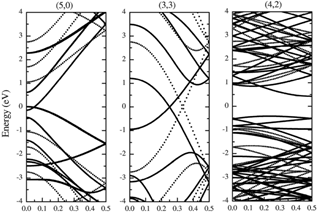
Figure 7. Calculated electronic band structure of nanotubes (5, 0), (3, 3) and (4, 2) from non-orthogonal tight-binding model in the energy range between −4 and 4 eV with respect to the Fermi energy. Dotted lines are results from the π-TB model with transfer integral γ0 = 2.75eV. Figure is taken from [20].
Okada et al [24] studied the curvature effect on electronic band structure of semiconducting SWCNTs. They found that optical transitions qualitatively differ from zone-folding calculation due to curvature. They also provided an explanation of the relative difference between optical transition energies of mod 1 and mod 2 type semiconducting SWCNTs based on curvature effect.
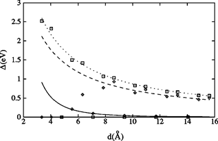
Figure 8. Band gaps of (4, 0) to (20, 0) zigzag tubes versus diameter. The squares show TB values, while the diamonds show DFT results. Figure is taken from [19].
Zolyomi et al [19] performed first-principles calculations of the electronic band structure of 40 different small diameter single-wall carbon nanotubes (9 armchairs, 17 zigzags, 14 chirals). They compared their calculated bandgaps to zone folding (ZF) tight binding (TB) values for all tubes. Significant differences were observed by them from what was expected from ZF-TB. Some of the ZF predicted semiconducting tubes proved to be metallic, due to σ-π mixing caused by high curvature, whereas eight of the ZF predicted metallic tubes (4 zigzags, 4 chirals) showed a small gap in the band structure. The Fermi wave-vector of armchair tubes showed a downshift from its ZF-expected value; this
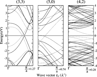
Figure 9. Solid line represents zone folding electronic band structures of the 4-Å SWNT’s. Dotted line represents ab initio electronic band structures of the relaxed 4-Å nanotubes. The Fermi level is at 0 ev. Figure is taken from [41].
shift was proportional to 1/d 2.
Bertoni et al [40] presented first principles calculations of the electronic structure of small carbon nanotubes with different chiral angles and different diameters (d<1 nm). They compared the band structure and density of states (DOS) of chiral nanotubes with those of zigzag and armchair tubes with similar diameters. They evaluated the degree of hybridization occurs in these small diameters tubes due to higher curvature.
Machon et al [41] and Yang et al [42] performed first principle calculation using local density function approximation (LDA) to study their optical properties of lowest diameter 0.4 nm SWCNT that refers to (4, 2), (3,3) and (5, 0) tubes. Li et al [43] also studied the structure of these tubes using transmission electron microscopy (TEM) and compared their observation with LDA calculations. LDA calculation of band structure of this smallest diameter tube showed that the chiral (4, 2) tube is a semiconductor with a small indirect band gap, armchair (3,3) is a metal, and zigzag (5, 0) is a metal, too, with a finite electronic density of state near the Fermi energy level [33]. Their conclusion that (5, 0) nanotube is metallic is in contrast to the prediction of the zone folding approximation which considered this tube to be a mod 2 type semiconducting tube. They explained this feature as an effect of the strong curvature of the nanotube walls.
Liang et al [44] performed similar calculation but with semi-empirical local density matrix (LDM) method to study around 0.4 nm SWCNTs i.e. (4, 2), (3,3) and (5,0) tubes. Additionally, they performed absorption spectroscopy on these tubes to verify their calculation. They found that, unlike those of the larger diameter CNTs whose absorption spectra are determined by their diameters, the absorption spectra of small diameter SWNTs such as (4, 2), (3,3) and (5,0) are sensitive to their chiralities as well as their diameters.
Generally, small diameter nanotubes require a more refined treatment beyond the simple tight-binding graphene model, as zone folding approximation may completely fail in those cases due to high curvature effect [38].
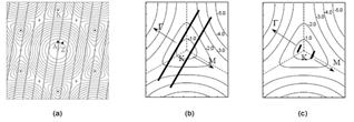
Figure 10. (a) Contour plot of the energy bands of graphene in hexagonal Brillouin zone of reciprocal space. The corners K of the first Brillouin zone are indicated by the black dots. Region near K point shows trigonal asymmetry. Figure is taken from [45]. The wavenumbers k (thick black lines) allowed by the periodic boundary condition along the circumference for (b) the (10,0) mod 1 tube and (c) the (9,1) mod 2 tube, near K point. Figure is taken from [24].
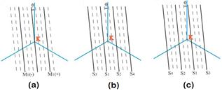
Figure 11. Zone-folding picture of carbon nanotubes around the K point in the Brillouin zone of graphene. The blue lines are the Brillouin zone boundary, and the angle φ is the deviation of the nanotube from the armchair direction. The solid lines spaced by a distance 2/dt represent the available states consistent with the boundary conditions for (a) metallic nanotubes with mod(n-m, 3) = 0 and semiconducting nanotubes with (b) mod(n-m, 3) = 1 and (c) mod(n-m, 3) = 2. Odd bands (S1, S3, ..) in (b) have lower energies than their counterparts in (c) for tubes of the same diameter, whereas even bands (S2, S4, ..) have higher energies. Figure is taken from [17].
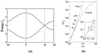
Figure 12. (a) Energy dispersion of graphene along high-symmetry points. (b) The energy dispersion along the K–Γ and K–M directions. The optical transition energies corresponding to the lowest 1D energy level are plotted for metallic (open circles) and semiconducting (closed circles) zigzag nanotubes (n, 0) by putting ka = |K1|a and ka = |K1|a/3, respectively. (The inset shows an expanded view of the Figure at small E/γ0 and small ka for semiconducting nanotubes.) Figure is taken from [36,46].
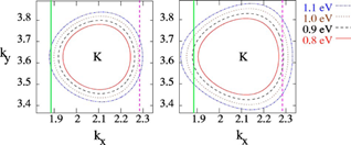
Figure 13. Equi-excitation-energy contours of graphene with TB (left side) and DFT (right side) around the K point (located at kx=2π/3 and ky=2π/3, in units of an inverse lattice constant). The solid (green) and dashed (purple) vertical lines correspond to those allowed k-lines of the (10, 0) and (11, 0) nanotubes, respectively, which are nearest to the K point, thus the k-lines which determine the value of the band gap of these zigzag tubes. Clearly, the trigonal warping effect is larger in the DFT calculation, than it is in the TB calculation. Figure is taken from [19].
3.2. Trigonal Warping Effect
The second factor is the ‘trigonal warping effect’ [17,19,24,34]. Reported deviations of TB model derived band structure and transition energies of nanotubes are not only due to the linearity of the graphene bands, but also due to their variation with directions in the Brillouin zone, termed as ‘trigonal warping’ [34]. Fig 10 shows Contour plot of the energy bands of graphene in reciprocal space where region around K point shows trigonal asymmetry instead of being circular. Due to this trigonal asymmetry near the six corners of Brilluine zone (asymmetric cone around K-point), difference in transition energies for mod 1 and mod 2 type semiconducting SWCNTs occurs. As shown in Fig 10 and Fig 11, odd transitions (E11S, E33S,….) and even transitions (E22S, E44S,….) for mod-1 and mod-2 type semiconducting SWCNTs lie on alternate sides of the K point [17]. In mod 1 type, the first transition (E11) comes from K – M direction and the second transition (E22) comes from K – Γ direction. In mod 2 type, this is reversed, i.e. the first transition comes from K – Γ direction and the second transition comes from K – M direction. As the transition energies in the K – Γ direction are larger than those at the same distance in the K – M direction, as seen from Fig. 12, the magnitude of the transition energies in mod 2 and mod 1 tubes alternates when going from E11 to E22.
This difference of transitions for mod 1 and mod 2 types also leads to a general prediction of earlier mentioned "family behavior", within the context of graphene zone folding model. Though zone folding provides an explanation of this trigonal warping and consequent energy difference, but, it cannot fully account it. Zolyomi et al [19] showed on the basis of their LDA calculation that trigonal warping effect found by their DFT calculation, is higher than that predicted by zone folding approach.
Saito et al [34] investigated the ‘trigonal warping effect’ analytically and derived expressions to estimate the corresponding deviation in optical transitions of metallic and semiconducting SWCNTs. They showed that trigonal warping causes splitting of the density of State (DOS) peaks of metallic SWCNTs except for armchair tubes.
Okada et al [24] reported the relative difference between optical transition energies of mod 1 and mod 2 type based on their calculation, and they explained it using same arguments given above.
Sfeir et al [17] provided a firm experimental basis for ‘trigonal warping effect’ and family behavior as they observed these from their Rayliegh scattering experimental. They also discussed the cause of relative difference between optical transition energies of mod 1 and mod 2 type for even and odd transitions.
3.3. Chirality Effect
The third factor is ‘chirality effect’ [9,33,44] that originates from individual nanotube chirality and results unique features for each tube. Dependence of band structure and transition energies of nanotubes on their precise chiral structure is discussed theoretically and also observed from many experiments [16,18,22,32,47,55].
Gulseren et al [32], Ding et al [33], Saito et al [34], Maultzsch et al [47], Yorikawa et al [48,53], and Jorio et al [52] –all discussed relation of nanotube band gaps to chirality and proposed chirality dependent term to be included with Eqn. (1) to account this effect. In fact, chirality effect in SWCNT is significant because it is embedded in rest other effects also. For example, the curvature effect is more dominant on zigzag (n, 0) and chiral tubes (n, m) than armchair tubes (n, n) [19].
Trigonal warping splits DOS of metallic tubes which is highest for metallic zigzag tubes, whereas no splitting for Semiconducting tubes [34]. Also, the upper and lower bounds of the widths of the optical transitions (Eii) curves alternate with increasing i between the mod 1 and mod 2 zigzag semiconducting SWCNTs. Smallest diameter zigzag tubes are more metallic than similar diameter ciral tubes [34]. It is also observed that, in experimental katura plot, chirality changes from armchair to zigzag along (2n+m) family lines [23]. Another family is observed in experimental E22/E11 plot where nanaotubes having same (n-m) values fall along same symmetric lines or family branches [18]. These families are directly linked with their chiral index values. Also, in case of blue shift of transition energies, tubes chirality near to armchair tubes are found at the border of the shifting [26]. All these clearly establish that band structure and transition energies of nanotubes shows unique features for different chiralities and indicate their dependency on chiral index (n, m) value of each tube. While curvature effect and trigonal effect are highly considered to heal up the limitations of simple TB model, chirality effect are comparatively less pronounced, despite its significance and impact on various electronics properties.
3.4. Many Body Effect
The fourth factor is many body effect (electron-electron interaction) [25-29,31,56,60], which can be further decomposed into an exciton binding energy and a self-energy. Kane et al [25], Mele et al [26], Lin et al [27], Spataru et al [28,59], Zhao et al [29], Dukovic et al [31], Samsonidze et al [22], Jiang et al [56], Sato et al [57], Ando et al [58], and Pedersen et al [59] studied the many body effect on electronic properties of SWCNTs. It is believed by some authors that the main explanation for the ‘ratio problem’ and ‘blue shift problem’ can be givn by showing the effect of many body ineteraction in SWCNTs [25-27,29,31], even if the relative contributions of self-energy and excitonic effects are not precisely known yet. The nature and amount of many body effects are still being discussed in literatures and also much disputed. Theories which include many particle interactions are still quite rare and time consuming. Therefore no complete Kataura plot has been provided so far which includes curvature effects, electron-electron and electron-hole interaction [35].
However, a recent study of Sato et al [57] showed that, for E11 and E22 transitions, the chirality dependence of the exciton binding energy for each (n,m) SWCNT is almost cancelled by that of the self energy, both effects being of the same order of magnitude, in the range of 0.5 to 1 eV [27]. Thus the origin of the family pattern for E11 and E22 can be understood by the chirality dependence of the single particle energies, by safely ignoring many body effect.
4. Conclusions
An in depth review of various theoretical and experimental research works on evaluation of Tight binding model in describing electronic band structure of Single Wall Carbon Nanotubes is presented in this work. It has been thoroughly discussed and showed that Tight binding model of SWCNTs, as obtained from simple linearized tight binding model of π-band of graphene with zone folding approximation has some limitations. It cannot give full qualitative and quantitative description of optical transition energies of SWCNTs, significantly deviates from experimental data and cannot account some experimental observation. For example, it underestimates and overestimates first and second optical transition energies, respectively, of semiconducting SWCNTs (E11S, E22S) around 25%. Its quantitative failure is more prominent for lower diameter tubes. It also fails to reflect relative difference between mod 1 and mod 2 type semiconducting SWCNTs for odd transitions (like, E11) and even transitions (like, E22) with comparable diameter and gives incorrect ratio of first two optical transitions, as observed from various optical spectroscopic experiments. This deviation is mainly attributed to ‘curvature effct’(due to nanotube curvature), ‘trigonal warping effect’ (due to trigonal asymmetry near the six corners of hexagonal Brilluine zone for SWCNTs), ‘chirality effect’ (due to unique chiral index of each SWCNT) and for many body effect (which is not significant if only E11 and E22 are considered). The conclusion from this work is, the simple linearized tight binding model fails to describe electronic band structure and corresponding transition energies of SWCNTs. Hence, an improved theoretical model need to be used for complete representation of the electronic and optical properties of SWCNTs. Alternatively, an intelligently devised empirical model can also be used that incorporate all the observations from various experiments reported so far.
References
- S. Iijima, "Helical microtubules of graphitic carbon", Nature 354, pp.56 – 58, 1991.
- S. Iijima and T. Ichihashi, "Single-shell carbon nanotubes of 1-nm diameter", Nature 363, pp.603 – 605, 1993.
- A. P. Graham, G.S. Duesberg, W. Hoenlein, F. Kreupl, M. Liebau, R. martin, B. Rajasekharan, W. Pamler, R. Seidel, W. Steinhoegl, E. Unger, "How Do Carbon Nanotubes Fit into the Semiconductor Roadmap?", Appl. Phys. A, 80, pp.1141–1151, 2005.
- Kahng, B. Andrew, "Scaling: More than Moore's law", Design and Test of Computers, IEEE, Vol. 27 , Issue 3, pp.86 – 87, 2010.V. N. Popov, "Carbon nanotubes : properties and application", Materials Science and Engineering R, 43, pp. 61–102, 2004.
- V. N. Popov, "Carbon nanotubes: properties and application", Materials Science and Engineering R, 43, pp. 61–102, 2004.
- T. W. Odom, J. L. Huang, P. Kim, and C. M. Lieber, "Structure and Electronic Properties of Carbon Nanotubes",J. Phys. Chem. B,104,pp.2794-2809, 2000.
- N. Hamada, S. Sawada, and A. Oshiyama, "New one-dimensional conductors: graphitic microtubules," Phys. Rev. Lett., Vol.68,No.10,pp.1579-1581, 1992.
- J. W. Mintmire and C. T. White, "Universal density of states for carbon nanotubes", Phys. Rev. Lett., Vol. 81, No.12, 1998.
- S. Reich and C. Thomsen, "Chirality dependence of the density-of-states singularities in carbon nanotubes", Phys. Rev. B, Vol 62, No. 7, 2000.
- M.S. Dresselhausa, G. Dresselhausc, A. Jorio, A.G. Souza Filho, R. Saito, "Raman spectroscopy on isolated single wall carbon nanotubes", Carbon, 40, pp.2043–2061, 2002.
- J. D. Correa, A. J. R. da Silva, and M. Pacheco, "Tight-binding model for carbon nanotubes from ab initio calculations," J. Phys.: Condens. Matter, Vol.22,No.7, 275503, 2010.
- R. Kundu, "Tight binding parameters for graphene", Modern Physics Letters B, Vol. 25, No. 3, pp.163-173, 2011.
- S. Reich, J. Maultzsch, and C. Thomsen, "Tight-binding description of graphene," Phys. Rev. B, Vol.66,No.3,pp.035412, 2002.
- Y. Lian, Y. Maeda, T. Wakahara, T. Akasaka, S. Kazaoui, N. Minami, N. Choi and H. Tokumoto, "Assignment of the Fine Structure in the Optical Absorption Spectra of Soluble Single-Walled Carbon Nanotubes", J. Phys. Chem. B, 107, 12082-12087, 2003.
- H. Kataura, Y. Kumazawa, Y. Maniwa, I. Umezu, S. Suzuki, Y. Ohtsuka, and Y.Achiba, "Optical properties of single-wall carbon nanotubes," Synthetic Met., Vol.103,pp.2555, 1999.
- R. B. Weisman and S. M. Bachilo, "Dependence of optical transition energies on structure for single-walled carbon nanotubes in aqueous suspension: an empirical kataura plot," Nano Lett., Vol.3,No.9,pp.1235-1238, 2003.
- M. Y Sfeir., T.Beetz, F Wang, L.Huang, X. M. H Huang., M.Huang, J. Hone, S. O’Brien, J. A Misewich, T. F.Heinz, L.Wu, Y.Zhu, L. E. Brus, " Optical Spectroscopy of Individual Single-Walled Carbon Nanotubes of Defined Chiral Structure", Science, Vol. 312, April 2006.
- Bachilo S. M., Strano M. S., Kittrell C., Hauge R. H., Smalley R. E., Weisman R. B., "Structure-Assigned Optical Spectra of Single-Walled Carbon Nanotubes", Science, Vol 298 No. 5602, pp.2361, 2002.
- V. Zólyomi and J. Kürti, "First-principles calculations for the electronic band structures of small diameter single-wall carbon nanotubes", Phys. Rev. B 70, 085403, 2004.
- V. N. Popov,"Curvature effects on the structural, electronic and optical properties of isolated single-walled carbon nanotubes within a symmetry-adapted non-orthogonal tight-binding model", New Journal of Physics, Vol. 6,2004.
- H. Zeng, H. F. Hu, J. W. Wei, Z. Y. Wang, L. Wang, and P. Peng, "Curvature effects on electronic properties of small radius nanotube," Appl. Phys. Lett., Vol.91,No.3,pp.033102, 2007.
- Ge. G. Samsonidze, R. Saito, N. Kobayashi, A. Grüneis, J. Jiang, A. Jorio, S. G. Chou, G. Dresselhaus and M. S. Dresselhaus, "Family behavior of the optical transition energies in single-wall carbon nanotubes of smaller diameters, Appl. Phys. Lett., Vol 85, No. 23, 2004.
- J. Maultzsch , C. Thomsen,"Characterization of Carbon Nanotubes by Optical Spectroscopy,Advanced Micro and Nanosystems", Carbon Nanotube Devices, Vol. 8.,Edited by Christofer Hierold, Verlag GmbH and Co. KGaA, Weinheim, Berlin, Germany, 2008.
- S. Okada, S. Ogawa, and S. Maruyama, "Curvature Effects on Electron States of Semiconducting Nanotubes", Materials Science, Feb 20, 2004.
- Kane C. L. and Mele E. J., "The Ratio Problem in Single Carbon Nanotube Fluorescence Spectroscopy", Phys. Rev. Lett. 90, 207401, 2003.
- E. J. Mele, C.L. Kane, "Many body effects in carbon nanotube fluorescence spectroscopy", Solid State Communications 135, pp. 527–531, 2005.
- H. Lin, J. Lagoute, V. Repain, C. Chacon, Y. Girard, J.-S. Lauret, F. Ducastelle, A. Loiseau S. Rousset , "Many-body effects in electronic bandgaps of carbon nanotubes measured by scanning tunnelling spectroscopy", Nature Materials 9, 235–238, 2010.
- C. D. Spataru, S. I. Beigi, L. X. Benedict and S. G. Louie, "Excitonic Effects and Optical Spectra of Single-Walled Carbon Nanotubes", AIP Conf. Proc., vol 772, p. 1061-1062, 2004.
- H. Zhao, S. Mazumdar, "Excitons in semiconducting single-walled carbon nanotubes", Synthetic Metals, 155, p.250–253, 2005.
- M. J. O'Connell, S.M. Bachilo, C.B. Huffman, V.C. Moore, M.S. Strano, E.H. Haroz, K.L. Rialon, P.J. Boul, W.H. Noon, C. Kittrell, J. Ma, R.H. Hauge, R.B. Weisman, and R.E. Smalley, "Band Gap Fluorescence from Individual Single-Walled Carbon Nanotubes", Science 297, pp.5581-5593, 2002.
- G. Dukovic, F. Wang, D. Song, M. Y. Sfeir, T. F. Heinz, and L. E. Brus, "Structural dependence of excitonic optical transitions and band-gap energies in carbon nanotubes," Nano Lett., Vol.5,No.11,pp.2314-2318, 2005.
- O. Gulseren, T. Yildirim and S. Ciraci,"A systematic ab-initio study of curvature effects in carbon nanotubes", Phys. Rev. B 65, 153405, 2002.
- J W Ding, X H Yan, J X Cao, "Analytical relation of band gaps to both chirality and diameter of single-wall carbon nanotubes", Phys. Rev. B , Vol. 66, Issue 7, Pages: 2-5, 2002.
- R. Saito, G. Dresselhaus, and M. S. Dresselhaus, "Trigonal warping effect of carbon nanotubes," Phys. Rev. B, Vol.61,No.4,pp.2981-2990, 2000.
- H. Telg, "Raman studies on individual nanotubes and nanotube ensembles –vibrational properties and scattering efficiencies", Ph.d thesis, Physics, Institute für Festkörperphysik,Berlin, 2009.
- A. Javey, J. Kong, Editors: "Carbon Nanotube Electronics", pp. 16, 35, Springer Science and Business Media, LLC, 2009.
- Ana Dergan, "Electronic and transport properties of carbon nanotubes", seminar paper, Department of physics, University of Ljubljana, October 2010.
- Francois Leonard, "The physics of carbon nanotube devices", Ed: Jeremy Ramsden, William Andrew Inc. Norwich, New York. 2009.
- C. L. Kane and E. J. Mele, "Size, shape, and low energy electronic structure of carbon nanotubes," Phys. Rev. Lett., vol. 78, pp. 1932–1935, 1997.
- G. Bertoni, L. Calmels, "First-principles calculation of the electronic structure and energy loss near edge spectra of chiral carbon nanotubes", Micron 37, pp.486–491, 2006.
- M. Machón, S. Reich, C. Thomsen, D. S. Portal and P. Ordejón, "Ab initio calculations of the optical properties of 4-Å-diameter single-walled nanotubes", Phys. Rev. B 66, 155410, 2002.
- X. P. Yang, H. M. Weng and J. Dong, "Optical properties of 4 Å single-walled carbon nanotubes inside the zeolite channels studied from first principles calculations", The European Physical Journal B - Condensed Matter and Complex Systems, Vol. 32, No. 3, pp.345-350, 2003.
- G.D. Li, Z.K. Tang, N. Wang, J.S. Chen, "Structural study of the 0.4-nm single-walled carbon nanotubes aligned in channels of AlPO4-5 crystal", Carbon, 40, pp.917–921, 2002.
- W. Z. Liang, G. Chen, Z. Li, Z. K. Tang, "Absorption spectra and chirality of single-walled 4 Å carbon nanotubes" , Applied Physics Letters, vol. 80 no. 18, pp. 3415-3417, 2002.
- P. Lambin, F. Troizon and V. Meunier, "Electronic Transport in Nanotubes and Through Junctions of Nanotubes", Carbon Nanotubes:NATO Science Series, Volume 222, III, pp. 123-142, 2006.
- R. Saito and H. Kataura, "Optical Properties and Raman Spectroscopy of Carbon Nanotubes", Carbon Nanotubes, Edited by M. S. Dresselhaus, G. Dresselhaus, Ph. Avouris,Topics in Applied Physics, Vol. 80, pp.213-247, Springer-Verlag Berlin Heidelberg, 2001.
- J. Maultzsch, H. Telg, S. Reich, and C. Thomsen, "Radial breathing mode of single-walled carbon nanotubes Optical transition energies and chiral-index assignment", Phys. Rev. B 72, 205438, 2005.
- H. Yorikawa, S. Muramatsu, "Electronic structure characteristic of carbon nanotubules",Z. Phys. B, Condensed Matt., vol. 104, pp. 71–76, 1997.
- A. Jorio, C. Fantini, M. A. Pimenta, R. B. Capaz ,Ge. G. Samsonidze, G. Dresselhaus, M. S. Dresselhaus, J. Jiang, N. Kobayashi, A. Grüneis and R. Saito, "Resonance Raman spectroscopy (n,m)-dependent effects in small-diameter single-wall carbon nanotubes", Phys. Rev. B 71, 075401, 2005.
- J. Lefebvre, S. Maruyama and P. Finnie, "Photoluminescence: science and applications", Topics in Applied Physics, Vol. 111, pp.287-319, 2008.
- P. K. Valavala, D. Banyai, M. Seel, and R. Pati, "Self-consistent calculations of strain-induced band gap changes in semiconducting (n,0) carbon nanotubes," Phys. Rev. B, Vol.78,No.23,pp.235430, 2008.
- A. Jorio, P. Araujo, S. K. Doorn, S. Maruyama, H. Chacham, and M. A. Pimenta, "The Kataura plot over broad energy and diameter ranges," Phys. Stat. Sol. (b), Vol.243,No.13,pp.3117-3121, 2006.
- H. Yorikawa and S. Muramatsu, "Energy gaps of semiconducting nanotubles," Phys. Rev. B, Vol.52,No.4,pp.2723-2727, 1995.
- H. Yorikawa and S. Muramatsu , "Chirality-dependence of energy gaps of semiconducting nanotubules" , Solid State Communications, Vol. 94, Issue 6, Pages 435-437, 1995.
- G. Lanzani, L. Luer, "Carbon Nanotubes: Electronic Structure and Spectroscopy", Comprehensive Nanoscience and Technology, Vol. 1, pp. 23–39, 2011.
- J. Jiang, R. Saito, Ge. G. Samsonidze, A. Jorio, S. G. Chou, G. Dresselhaus and M. S. Dresselhaus, "Chirality dependence of exciton effects in single-wall carbon nanotubes: Tight-binding model", Phys. Rev. B 75, 035407, 2007.
- K. SatoaR. Saito,J. Jiang, G. Dresselhaus, M.S. Dresselhaus, "Chirality dependence of many body effects of single wall carbon nanotubes", Vibrational Spectroscopy:Elsevier,Vol. 45, Issue 2, pp.89–94, 2007.
- T. Ando, "Family Effects on Excitons in Semiconducting Carbon Nanotubes" Journal of the Physical Society of Japan, Vol. 78, No. 10, 104703, 2009.
- T. G. Pedersen, "Exciton effects in carbon nanotubes", Carbon 42, pp.1007–1010, 2004.
- C. D. Spataru,S. I. Beigi,R. B. Capaz,and S. G. Louie, "Theory and ab initio calculation of radiative lifetime of excitons in semiconducting carbon nanotubes",Phys. Rev. Lett.,vol. 95, Issue 24, 247402, 2005.


