
International Journal of Energy Science and Engineering, Vol. 1, No. 1, March 2015 Publish Date: Mar. 14, 2015 Pages: 1-12
Research on Unipolar Inverted Sine Carrier PWM Strategies for Three Phase Five Level CMLI
C. R. Balamurugan1, *, S. P. Natarajan2, R. Bensraj2, T. S. Anandhi2
1Department of EEE, Arunai Engineering College, Tiruvannamalai, Tamil nadu, India
2Department of EEE & EIE, Annamalai University, Chidambaram, Tamil nadu, India
Abstract
This paper presents the comparison of various Unipolar Inverted Sine Carrier Pulse Width Modulation (UISCPWM) techniques for the three phase Cascaded Multi Level Inverter (CMLI). Due to switch combination redundancies, there are certain degrees of freedom to generate the multilevel AC (Alternating Current) output voltage. This paper presents the use of Control Freedom Degree (CFD) combination. The effectiveness of the pulse width modulation strategies developed using CFD are demonstrated using simulation. The results indicate that the chosen five level inverter triggered by the developed UISCPSPWM (Unipolar Inverted Sine Carrier Phase Shift Pulse Width Modulation) and UISCVFPWM (Unipolar Inverted Sine Carrier Variable Frequency Pulse Width Modulation) strategy with sine and stepped wave reference and UISCAPODPWM strategy with 60 degree reference exhibits reduced harmonics and UISCCOPWM (Unipolar Inverted Sine Carrier Carrier Overlapping Pulse Width Modulation) provides higher fundamental RMS (Root Mean Square) output voltage for all references. Simulation are performed using MATLAB-SIMULINK.
Keywords
ISCPWM, CMLI, THD, 60 Degree, FF, Unipolar
Received: February 15, 2015
Accepted: March 7, 2015
Published online: March 12, 2015
@ 2015 The Authors. Published by American Institute of Science. This Open Access article is under the CC BY-NC license. http://creativecommons.org/licenses/by-nc/4.0/
Contents
1. Introduction 2. Multilevel Inverter 3. Unipolar Multi Carrier PWM Strategies 3.1. Unipolar Inverted Sine Carrier Phase Disposition PWM (UISCPDPWM) strategy 3.2. Unipolar Inverted Sine Carrier Alternative Phase Opposition and Disposition PWM (UISCAPODPWM) strategy 3.3. Unipolar Inverted Sine Carrier Phase Shift PWM (UISCPSPWM) strategy 3.4. Unipolar Inverted Sine Carrier Carrier Overlapping PWM (UISCCOPWM) strategy 3.5. Unipolar Inverted Sine Carrier Variable Frequency PWM (UISCVFPWM) Strategy 4. Inverted Sine PWM Technique for MLI 5. 60 Degree PWM Reference 6. Stepped Wave Reference 7. Simulation Results 7.1. Simulation Results for Sinusoidal Reference 7.2. Simulation Results for 60 Degree PWM Technique 7.3. Simulation Results for Stepped Wave PWM Technique 8. Conclusion
1. Introduction
The multilevel inverter topology gives the advantages of usage in high power and high voltage application with reduced harmonic distortion without a transformer. The semiconductor devices are not connected in series to for one single high-voltage switch. In which each group of devices contribute to a step in the output voltage waveform. The steps are increased to obtain an almost sinusoidal waveform. The number of switches involved is increased for every level increment. Donald Grahame Holmes and McGrath [1] proposed opportunities for harmonic cancellation with carrier based PWM for two level and multilevel cascaded inverters. Loh et al in [2] introduced synchronization of distributed PWM cascaded multilevel inverter with minimal harmonic distortion and common mode voltage. Mariethoz and Rufer [3] analysed resolution and efficiency improvements for three phase cascaded multilevel inverters. Xianglian Xu et al in [4] proposed phase shift SPWM (Sinusoidal Pulse Width Modulation) technique for cascaded multilevel inverter. Azli and Choong [5] analyzed the performance of a three phase cascaded H-bridge multilevel inverter. Shanthi and Natarajan proposed carrier overlapping PWM methods for single phase cascaded five level inverter [6]. Roozbeh Naderi and Rahomati [7] proposed phase shifted carrier PWM technique for general cascaded inverters. Gierri Waltrich and Barbi [8] introduced three phase cascaded multilevel inverter using power cells. Urmila and Subbarayudu [9] analyzed comparative study of various pulse width modulation techniques. Gierri Waltrich and Barbi [10] introduced also three phase cascaded multilevel inverter with commutation sub-cells. Konstantinou et al [11] proposed harmonic elimination control of a five level DC (Direct Current)-AC cascaded H-bridge hybrid inverter. Farid Khoucha et al [12] proposed comparison of symmetrical and asymmetrical three phase H-bridge multilevel inverter for direct torque control induction motor drives. Simulations are performed using MATLAB-SIMULINK. hhhhhHHarmonic analysis and evaluation of performance measures for various modulation indices have been carried out and presented.
2. Multilevel Inverter
The concept of this inverter is based on connecting H-bridge inverters in series to get a sinusoidal voltage output. The output voltage is the sum of the voltage that is generated by each cell. The number of output voltage levels are 2n+1, where n is the number of cells. The switching angles can be chosen in such a way that the total harmonic distortion is minimized. One of the advantages of this type of multilevel inverter is that it needs less number of components comparative to the diode clamped or the flying capacitor, so the price and the weight of the inverter is less than that of the two former types. Fig. 1 shows a configuration of the three phase five level cascaded multilevel inverter. A cascaded multilevel inverter consists of a series of H-bridge inverter units. The general function of this inverter is to synthesize a desired voltage from several Separate DC Sources (SDCSs).
The load voltage is equal to the summation of the output voltage of the respective modules that are connected in series. The number of modules (M) which is equal to the number of DC sources required depend on the total number of positive, negative and zero levels (m) of the CMLI. It is usually assumed that m is odd as this would give an integer valued M. In this work, load voltage consists of five levels which include +2VDC, +VDC, 0, -VDC and -2VDC and the number of modules needed is 2. The following equation gives the relation between M and m. Where M= (m-1)/2.
The gate signals for chosen five level cascaded inverter are simulated using MATLAB-SIMULINK. The gate signal generator model developed is tested for various values of modulation index ma and for various PWM strategies. Fig. 2 shows a sample SIMULINK model developed for UISCPD (Unipolar Inverted Sine Carrier Phase Disposition) PWM method. The simulation results presented in this work in the form of the outputs of the chosen MLI are compared and evaluated.
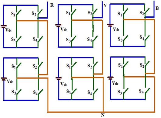
Fig. 1. A model set for a three phase cascaded five level inverter
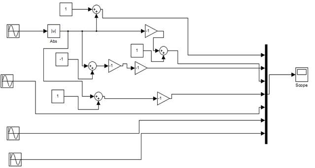
Fig. 2. Sample PWM generation logic using SIMULINK model developed for UISCPDPWM technique
3. Unipolar Multi Carrier PWM Strategies
This paper presents four types of unipolar PWM strategies. The reference in the unipolar strategy may be a rectified sinusoid or two sine references (sine and 1800 phase shifted sine) The later is used in this work. The multi carriers are positioned above zero level.
For an m-level inverter using unipolar multi-carrier technique, (m-1)/2 carriers with the same frequency fc and same peak-to-peak amplitude Ac are used. The reference waveform has amplitude Am and frequency fm and it is placed at the zero reference. The reference wave is continuously compared with each of the carrier signals. If the reference wave is more than a carrier signal, then the active devices corresponding to that carrier are switched on [10]. Otherwise, the device switches off. The frequency ratio mf is defined in the unipolar PWM strategy as follows:
![]() (1)
(1)
In this paper, mf = 40 and ma is varied from 0.6 to 1.
mf is chosen as 40 as a trade off in view of the following reasons:
(i) to reduce switching losses (which may be high at large mf)
(ii) to reduce the size of the filter needed for the closed loop control, the filter size being moderate at moderate frequencies.
(iii) to effectively utilise the available dSPACE system for hardware implementation.
3.1. Unipolar Inverted Sine Carrier Phase Disposition PWM (UISCPDPWM) strategy
The principle of the UISCPDPWM strategy is to use several triangular carriers with two modulation waves. For an m-level inverter, (m-1)/2 triangular carriers of the same frequency fc and the same peak-to-peak amplitude Ac are disposed so that the bands they occupy are contiguous [10]. The carrier set is placed above the zero reference.
![]() (2)
(2)
where n is the number of carriers
Carrier arrangements for five level UISCPDPWM are shown in Fig. 3 for ma=0.8.
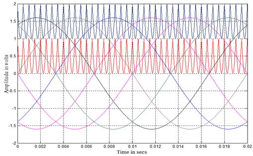
Fig. 3. Carrier arrangements for UISCPDPWM strategy (ma = 0.8, mf = 40)
3.2. Unipolar Inverted Sine Carrier Alternative Phase Opposition and Disposition PWM (UISCAPODPWM) strategy
Carriers are arranged in such a manner that each carrier is out of phase with its neighbour by 180 degrees (Fig.4).
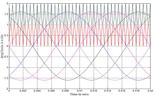
Fig. 4. Carrier arrangements for UISCAPODPWM strategy (ma = 0.8, mf = 40)
3.3. Unipolar Inverted Sine Carrier Phase Shift PWM (UISCPSPWM) strategy
The UISCPSPWM uses two carrier signals of same amplitude and frequency which are phase shifted by 900 to one another to generate the five level inverter output voltage. The gate signals for the CMLI are derived by comparison of the carriers with two sinusoidal references. The amplitude modulation index is defined for this strategy as follows:
![]() (3)
(3)
Carriers for five level inverter with UISCPSPWM strategy are illustrated in Fig. 5 for ma=0.8.
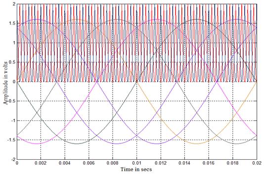
Fig. 5. Carrier arrangements for UISCPSPWM strategy (ma = 0.8 , mf = 40 )
3.4. Unipolar Inverted Sine Carrier Carrier Overlapping PWM (UISCCOPWM) strategy
The UISCCOPWM has two carriers’ signals of peak-to-peak amplitude Ac and they overlap with each other. The gate signals for this strategy are derived by comparing the two overlapping carriers with the two sine references [10]. Fig. 5 shows the carrier arrangements for the chosen MLI with UISCCOPWM strategy.
 (4)
(4)
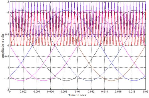
Fig. 6. Carrier arrangements for UISCCOPWM strategy (ma = 0.8, mf = 40)
3.5. Unipolar Inverted Sine Carrier Variable Frequency PWM (UISCVFPWM) Strategy
The number of switching for upper and lower devices of chosen MLI is much more than that of intermediate switches in PDPWM using constant frequency carriers. In order to equalize the number of switching for all the switches, variable frequency PWM strategy is used as illustrated in Fig. 6.
![]() (6)
(6)
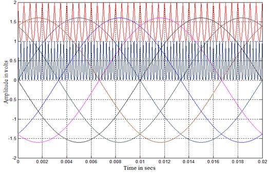
Fig. 7. Carrier arrangements for UISCVFPWM strategy (ma=0. , mf=40 for Upper and Lower Switches and mf = 80 for Intermediate Switches)
4. Inverted Sine PWM Technique for MLI
The inverted sine carrier PWM method uses the conventional sinusoidal reference signal and inverted sine carriers. The control scheme uses an inverted sine carrier that helps to maximize the output voltage for a given modulation index. For an ‘m’ level inverter, (m-1) carrier waves are required for bipolar PWM. The pulses are generated when the amplitude of the modulating signal is greater than that of the carrier signal[12,4].
The advantages of ISCPWM method are:
(i) It has a better spectral quality and a higher fundamental component compared to the conventional sinusoidal PWM without any pulse dropping.
(ii) The ISCPWM strategy enhances the fundamental output voltage particularly at lower modulation index ranges.
(iii) There is reduction in the total harmonic distortion and switching losses.
(iv) The appreciable improvement in the total harmonic distortion in the lower range of modulation index attracts drive applications where low speed operation is required.
(v) To increase the fundamental amplitude in the sinusoidal pulse width modulation the only way is by increasing the modulation index beyond 1 which is called over modulation. Over modulation causes the output voltage to contain many lower order harmonics and also makes the fundamental component Vs modulation index relation non-linear. Inverted sine pulse width modulation technique replaces over modulation.
This paper focuses on inverted sine carrier based sinusoidal PWM strategies and third harmonic injection PWM strategies which have been developed for the chosen three phase cascaded MLI.
5. 60 Degree PWM Reference
This method is almost similar to sinusoidal PWM except that the modulating sine wave is flat topped for a period of 60 degree in each half cycle [11]. 60 degree PWM reference technique is as shown in Fig. 8.
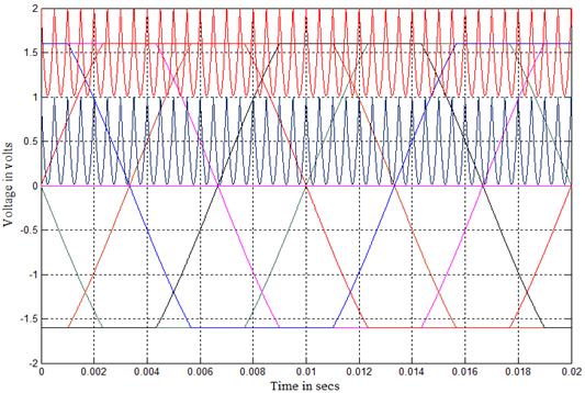
Fig. 8. Carrier arrangements for UISCPDPWM strategy (ma = 0.8, mf = 40)
6. Stepped Wave Reference
The stepped wave is not a sampled approximation to the sine wave. It is divided into specified intervals (say 200) with each interval controlled individually to control magnitude of the fundamental component and to eliminate specific harmonics. This type of control gives low distortion but higher fundamental amplitude compared with that of normal PWM control [11]. Stepped wave PWM techniques are as shown in Fig. 9.
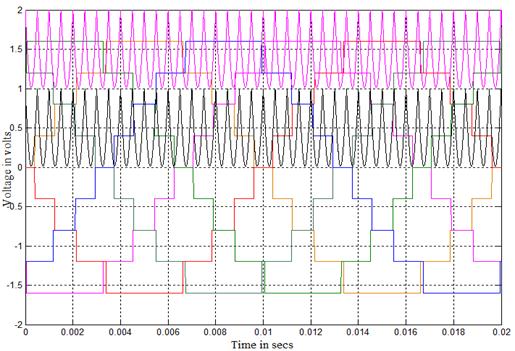
Fig. 9. Carrier arrangements for UISCPDPWM strategy (ma = 0.8, mf = 40)
7. Simulation Results
The cascaded five level inverter is modeled in SIMULINK using power system block set. Switching signals for CMLI are developed using unipolar inverted sine carrier PWM techniques discussed previously. Simulations are performed for different values of ma ranging from 0.6 – 1. The corresponding %THD (Total Harmonic Distortion) values are measured using FFT block and they are shown in Tables 1, 3 and 5. Tables 2, 4 and 6 display the VRMS of fundamental of inverter output for same modulation indices. Figs. 18 - 47 show the simulated output voltages of CMLI and corresponding FFT (Fast Fourier Transform) plots with above strategies but for only one sample value of ma = 0.8. Figs. 10 and 11 are for sine reference. Fig. 10 shows the five level output voltage generated by UISCPDPWM strategy and its FFT plot is shown in Fig. 11. From Fig. 11, it is observed that the UISCPDPWM strategy produces significant 7th, 9th, 31st, 33rd and 37th harmonic energy. It is observed that the UISCAPODPWM produces significant 3rd,5th, 9th, 31st, 35th, 37th and 39th harmonic energy. It is also observed that the UISCCOPWM strategy produces no significant/dominant harmonic. It is shown that the UISCPSPWM strategy produces significant 3rd, 5th and 7th harmonic energy. It is also shown that the UISCVFPWM strategy produces significant 7th , 9th, 35th and 39th harmonic energy.
The next two figures show results for 60 degree PWM strategy. Fig. 12 shows the five level output voltage generated by UISCPDPWM (60 degree) strategy and its FFT plot is shown in Fig. 13. From Fig. 13, it is observed that the UISCPDPWM (60 degree) strategy produces significant 3rd, 11th, 27th, 29th and 37th harmonic energy. It is observed that the UISCAPODPWM (60 degree) strategy produces significant 3rd, 5th, 7th, 27th, 31st, 33rd and 35th harmonic energy. It is also observed that the UISCCOPWM (60 degree) strategy produces significant 3rd and 37th harmonic energy. It is shown that the UISCPSPWM (60 degree) strategy produces significant 3rd and 5th harmonic energy. It is also shown that the UISCVFPWM (60 degree) strategy produces significant 3rd and 11th harmonic energy.
The next two figures show results for stepped wave PWM strategy. Fig. 14 shows the five level output voltage generated by UISCPDPWM (stepped wave) strategy and its FFT plot is shown in Fig. 15. From Fig. 15, it is observed that the UISCPDPWM (stepped wave) strategy produces significant 15th, 21st, 23rd, 25th, 31st and 37th harmonic energy. It is observed that the UISCAPODPWM (stepped wave) strategy produces significant 3rd, 5th, 11th, 15th, 19th, 25th, 27th, 29th, 31st, 33rd, 35th and 37th harmonic energy. It is also observed that the UISCCOPWM (stepped wave) strategy produces significant 3rd, 7th, 9th, 21st, 23rd, 25th and 29th harmonic energy. It is displayed that the UISCPSPWM (stepped) strategy produces significant 3rd, 5th, 7th, 21st, 23rd and 25th harmonic energy. It is also observed that the UISCVFPWM (stepped wave) strategy produces significant 3rd, 11th, 15th, 23rd, 25th, 27th and 35th harmonic energy. The following parameter values are used for simulation: VDC =220V and R (load) = 100 ohms.
7.1. Simulation Results for Sinusoidal Reference
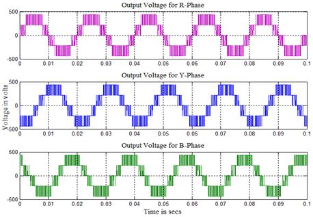
Fig. 10. Output voltage generated by UISCPDPWM strategy
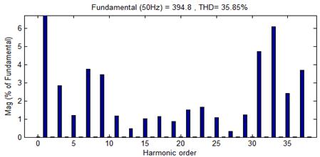
Fig. 11. Carrier arrangements for UISCVFPWM strategy (ma=0.8, mf=40 for Upper and Lower Switches and mf = 80 for Intermediate Switches)
7.2. Simulation Results for 60 Degree PWM Technique
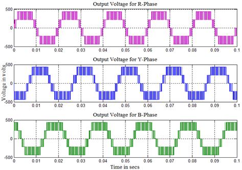
Fig. 12. Output voltage generated by UISCPDPWM strategy
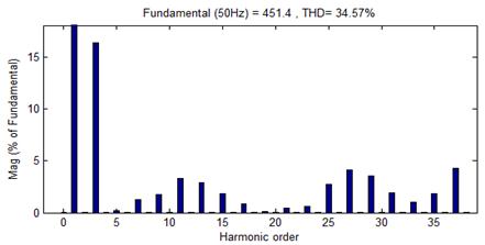
Fig. 13. FFT plot for output voltage of UISCPDPWM strategy
7.3. Simulation Results for Stepped Wave PWM Technique
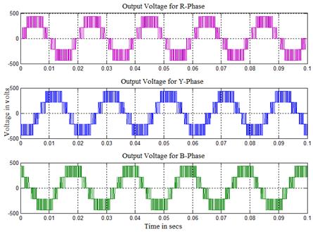
Fig. 14. Output voltage generated by UISCPDPWM strategy
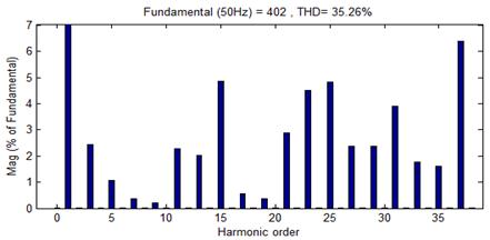
Fig. 15. FFT plot for output voltage of UISCPDPWM strategy
Table 1. % THD for different modulation indices with sinusoidal reference
| ma | UISCPD | UISCAPOD | UISCCO | UISCPS | UISCVF |
| 1 | 26.74 | 26.85 | 37.20 | 28.76 | 26.46 |
| 0.9 | 30.97 | 32.84 | 40.89 | 32.05 | 30.87 |
| 0.8 | 35.85 | 37.90 | 48.26 | 35.79 | 35.91 |
| 0.7 | 40.08 | 44.53 | 58.12 | 38.43 | 40.27 |
| 0.6 | 44.87 | 52.58 | 68.97 | 40.45 | 44.38 |
Table 2. VRMS (fundamental) for different modulation indices with sinusoidal reference
| ma | UISCPD | UISCAPOD | UISCCO | UISCPS | UISCVF |
| 1 | 328.7 | 322.5 | 342.2 | 338.1 | 328.9 |
| 0.9 | 304.7 | 295.7 | 325.2 | 318.5 | 304.8 |
| 0.8 | 279.1 | 268.5 | 301.7 | 296.8 | 278.6 |
| 0.7 | 249.8 | 234.6 | 275 | 275.1 | 249.5 |
| 0.6 | 213.6 | 191.7 | 244.3 | 253.7 | 214 |
Table 3. % THD for different modulation indices with 60 degree PWM reference
| ma | UISCPD | UISCAPOD | UISCCO | UISCPS | UISCVF |
| 1 | 25.74 | 24.64 | 33.16 | 28.73 | 25.57 |
| 0.9 | 31.19 | 29.91 | 36.95 | 32.57 | 31.00 |
| 0.8 | 34.57 | 34.42 | 40.46 | 38.02 | 34.54 |
| 0.7 | 39.54 | 39.44 | 51.11 | 39.46 | 39.64 |
| 0.6 | 42.20 | 43.11 | 61.57 | 43.07 | 42.13 |
Table 4. VRMS (fundamental) for different modulation indices with 60 degree PWM reference
| ma | UISCPD | UISCAPOD | UISCCO | UISCPS | UISCVF |
| 1 | 370.6 | 367.7 | 375.3 | 371.6 | 370.6 |
| 0.9 | 343.2 | 340.8 | 359 | 352.1 | 343.4 |
| 0.8 | 319.2 | 313.7 | 341.2 | 323.6 | 319.2 |
| 0.7 | 289.7 | 283.5 | 311.7 | 306.7 | 289.4 |
| 0.6 | 257.2 | 248.1 | 278.1 | 277.8 | 257.3 |
Table 5. % THD for different modulation indices with stepped wave reference
| ma | UISCPD | UISCAPOD | UISCCO | UISCPS | UISCVF |
| 1 | 21.79 | 23.23 | 36.18 | 26.88 | 22.01 |
| 0.9 | 29.33 | 32.90 | 40.76 | 30.50 | 29.02 |
| 0.8 | 35.26 | 38.85 | 43.87 | 34.99 | 34.92 |
| 0.7 | 39.30 | 43.02 | 54.42 | 36.36 | 39.65 |
| 0.6 | 42.60 | 56.73 | 65.61 | 38.21 | 42.32 |
Table 6. VRMS (fundamental) for different modulation indices with stepped wave reference
| ma | UISCPD | UISCAPOD | UISCCO | UISCPS | UISCVF |
| 1 | 330.3 | 327.2 | 344.7 | 336.6 | 330.9 |
| 0.9 | 307.1 | 299.5 | 325.6 | 319.2 | 309 |
| 0.8 | 284.2 | 275.6 | 303.9 | 296.8 | 285.7 |
| 0.7 | 249 | 239 | 275.9 | 280.7 | 249.9 |
| 0.6 | 216 | 190.5 | 245.9 | 252.1 | 217.2 |
Table 7. Crest factor for different modulation indices with sinusoidal reference
| ma | UISCPD | UISCAPOD | UISCCO | UISCPS | UISCVF |
| 1 | 1.4140 | 1.4142 | 1.4140 | 1.4140 | 1.4144 |
| 0.9 | 1.4145 | 1.4139 | 1.4142 | 1.414 | 1.4143 |
| 0.8 | 1.4145 | 1.4141 | 1.4143 | 1.4140 | 1.4142 |
| 0.7 | 1.4143 | 1.4143 | 1.4138 | 1.4143 | 1.4144 |
| 0.6 | 1.4143 | 1.4141 | 1.4142 | 1.4138 | 1.4144 |
Table 8. Crest factor for different modulation indices with 60 degree PWM reference
| ma | UISCPD | UISCAPOD | UISCCO | UISCPS | UISCVF |
| 1 | 1.4141 | 1.4141 | 1.4140 | 1.4141 | 1.4144 |
| 0.9 | 1.4143 | 1.4143 | 1.4142 | 1.4140 | 1.4140 |
| 0.8 | 1.4141 | 1.4144 | 1.4141 | 1.4144 | 1.4144 |
| 0.7 | 1.4142 | 1.4141 | 1.4141 | 1.4144 | 1.4143 |
| 0.6 | 1.4144 | 1.4143 | 1.4142 | 1.4143 | 1.4143 |
Table 9. Crest factor for different modulation indices with stepped wave reference
| ma | UISCPD | UISCAPOD | UISCCO | UISCPS | UISCVF |
| 1 | 1.4144 | 1.4144 | 1.4139 | 1.4144 | 1.4143 |
| 0.9 | 1.4141 | 1.4143 | 1.4143 | 1.4141 | 1.4142 |
| 0.8 | 1.4144 | 1.4136 | 1.4139 | 1.4140 | 1.4144 |
| 0.7 | 1.4140 | 1.4142 | 1.4139 | 1.4139 | 1.4141 |
| 0.6 | 1.4143 | 1.4141 | 1.4143 | 1.4141 | 1.4139 |
Table 10. Form factor for different modulation indices with sinusoidal reference
| ma | UISCPD | UISCAPOD | UISCCO | UISCPS | UISCVF |
| 1 | INF | INF | INF | INF | INF |
| 0.9 | INF | INF | INF | INF | INF |
| 0.8 | INF | INF | INF | INF | INF |
| 0.7 | INF | INF | INF | INF | INF |
| 0.6 | INF | INF | INF | INF | INF |
Table 11. Form factor for different modulation indices with 60 degree PWM reference
| ma | UISCPD | UISCAPOD | UISCCO | UISCPS | UISCVF |
| 1 | INF | INF | INF | INF | INF |
| 0.9 | INF | INF | INF | INF | INF |
| 0.8 | INF | INF | INF | INF | INF |
| 0.7 | INF | INF | INF | INF | INF |
| 0.6 | INF | INF | INF | INF | INF |
Table 12. Form factor for different modulation indices with stepped wave reference
| ma | UISCPD | UISCAPOD | UISCCO | UISCPS | UISCVF |
| 1 | INF | INF | INF | INF | INF |
| 0.9 | INF | INF | INF | INF | INF |
| 0.8 | INF | INF | INF | INF | INF |
| 0.7 | INF | INF | INF | INF | INF |
| 0.6 | INF | INF | INF | INF | INF |
8. Conclusion
It is observed from Tables 1, 3 and 5 that UISCAPODPWM with 60 degree PWM reference provide output with low distortion and UISCPSPWM and UISCVFPWM with sine and stepped wave reference provide output with relatively low distortion. UISCCOPWM with sine, 60 degree and stepped wave references is found to perform better since it provides relatively higher fundamental RMS output voltage (Tables 2, 4 and 6). Tables 7, 8 and 9 provide crest factor and Tables 10, 11 and 12 provide FF for all modulating indices. Depending on the performance measure required in a particular application of chosen MLI based on the output quality appropriate PWM have to be employed.
References
- Donald Grahame Holmes and Brendam P. Mcgrath, Opportunities for harmonic Cancellation with carrier based PWM for two-level and multilevel cascaded inverters, In: IEEE Trans. Industry Applications. vol.37, no.2, 2001, pp. 574-582.
- P.C.Loh, D.G.Holme and T.A.Lipo, Synchronization of distributed PWM cascaded multilevel inverter with minimal harmonic distortion and common mode voltage. In: IEEE Conf.Rec:0-7803-7754-0/03, 2003, pp.177-182.
- S.Mariethoz and A.Rufer, Resolution and efficiency improvements for three phase cascaded multilevel inverters In: IEEE Conf. Rec: 0-7803-8399-0/04, 2004, pp.4441-4446.
- Xianglian Xu, Yunping Zou, Kai Ding and Feiliu, Cascaded multilevel inverter with phase-shift SPWM and its application in STATCOM, In: IEEE Conf. Rec: 0-7803-8730-9/04, 2004, pp. 1139-1143.
- N.A.Azhi and Y.C.Choong, Analysis on the performance of a three phase cascaded H-Bridge multilevel Inverter, In: IEEE Conf. Rec: 1-4244-0273-5/06, 2006, pp. 405-410.
- B.Shanthi and S.P.Natarajan, Carrier overlapping PWM methods for single phase cascaded five level inverter, International Journal of Science and Technology of Automatic Control & Computer engineering (IJ-STA, Tunisia), Special issue on Control of Electrical Machines, 2008, pp.590-601.
- Roozbeh Naderi and Abdolreza Rahmati, Phase-shifted carrier PWM technique for general cascaded inverters, In: IEEE Trans. Power Electronics, 23(3), 2008, pp.1257-1269.
- Gierri Waltrich and Ivo Barbi, Three-phase cascaded multilevel inverter using power cell switch with two inverter legs in series, In: IEEE Trans. Industrial Electronics, 57(8), 2010, pp.2605-2612.
- B.Urmila and D.Subbarayudu, Multilevel Inverters: A comparative study of pulse width modulation techniques, Journal of Scientific & Engineering Research, 1(3), 2010, pp.1-5.
- [Gierri waltrich and Ivo Barbi, Three-phase cascaded multilevel inverter using commutation sub-cells, In: IEEE Conf.Rec.978-1-4244-3370-4/09, 2010, pp.362-368.
- Georgious S.Konstantinou, Sridhar R.Pulikanti and Vassilios G.Agalidis, Harmonic elimination control of a five level DC-AC cascaded H-bridge hybrid inverter, In: 2nd IEEE International Symposium on Power Electronics for Distributed Generation Systems. Rec. 978-1-4244-5670-3, 2010, pp.352-357.
- Farid khoucha and Mouna Soumia Lagoun, Adelaziz Kheloui and Mohamed EI Hachemi Benbouzid, A comparision of symmetrical and asymmetrical Three-phase H-Bridge multilevel inverter for DTC Induction motor drives, IEEE Trans. Energy Conversion, 26(1), 2011, pp.64-72.


