
International Journal of Materials Chemistry and Physics, Vol. 1, No. 2, October 2015 Publish Date: Aug. 27, 2015 Pages: 182-188
A Transient Study for SAW Propagation upon GaAs Substrate
M. M. Elsherbini1, *, M. F. Elkordy2, A. M. Gomaa1
1Dept. of Electrical Engineering, Shoubra Faculty of Engineering, Benha University, Cairo, Egypt
2Dept. of Communications, Faculty of Electronic Engineering, Menoufia University, Menouf, Egypt
Abstract
A SAW delay line is modelled with Finite element modelling technique upon A Gallium arsenide substrate and this device is modelled and simulated around center frequency of 1.5GHz that is used in different electronic devices at a high frequency range. A five periodic cycles of output voltage is simulated and monitored at output port of delay line while applying a sine wave to input port. Displacement of the SAW through the thickness of piezoelectric substrate is recorded and proofed that SAW doesn't penetrate more than the designed thickness. Displacement along wave direction is also monitored.
Keywords
FEM SAW, Delay Line, RF
Received: August 11, 2015
Accepted: August 17, 2015
Published online: August 27, 2015
@ 2015 The Authors. Published by American Institute of Science. This Open Access article is under the CC BY-NC license. http://creativecommons.org/licenses/by-nc/4.0/
1. Introduction
Acoustic wave devices shown in figure (1) based upon wave generated on the surface of a piezoelectric substrate like Quartz, GaAs, LiNaBo3, LiTaO3, etc.
SAW delay line structure have three ports, two of them are acoustic; one Input and the other is for output and the third is for electric port. Each port of two acoustics is consists of IDT structure with many fingers spaced as a function of wavelength, one acts as a transmitter (input port) that converts electrical signal into electromechanical wave propagates on the surface of piezoelectric material. The travel length between receiver and transmitter IDT is called as Delay Time. IDTs have a comb-like structure, where the distance between the fingers in the IDT determines the frequency of the waves propagating over the substrate.
The study of these waves is useful in seismology and other areas. The piezoelectric effect is a deflection induced by a voltage across the substrate material or a voltage created by deflection across the material [1].
Rayleigh waves (SAW) have two components, longitudinal and vertical shear components, they couple with a media in contact with the surface and affect the amplitude and velocity of the wave. This allow SAW device to sense mechanical properties.
SAW devices found in many applications like filters, oscillators, and transformers based on transmission the acoustic wave between input and output ports. Each port employs one or more IDTs (inter-digital transducers) to convert between electrical signals and acoustic (electromechanical) wave and vice versa using piezoelectric effect. More deep applications are now found using SAW devices in Radio, TV, Geophysics, Microfluidics, Flow measurement and Military uses [2]. Some previous simulation attempts for SAW devices like filters and correlators are illustrated in frequency domain [3] [4] [5]. Other study for frequency domain analysis for SAW delay line is introduced [6].
Finite Element Modelling (FEM) is the most numerical representation of field theory where the piezoelectric characteristics of the SAW devices can be easily recorded [7]. FEM tools also provide 2D and 3D view for SAW device, such as COMSOL and ANSYS [8-9].
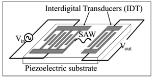
Figure (1). SAW delay line [10].
2. Substrate Selection
GaAs, gallium arsenide is selected in order to its electronic properties like higher speed switching in semiconductor devices. Also in SAW devices, it has large mobility of electrons. GaAs rarely affect with high temperature (overheating) because it has wide energy band. Devices made of GaAs can operate at frequencies more than 250GHz. It also generates a very low noise in the circuit with high device frequency.
For all above specifications, GaAs can be used in many applications like mobile phones, satellite, radar systems, and solar detectors [11].
From the basics of SAW, it is known that SAW propagation in a piezoelectric substrate is controlled through both stress and strain equation (electromechanical) of motion [12].
![]() (1)
(1)
![]() (2)
(2)
T is the stress matrix, S is the strain tensors, E is the electric potential field and D is the displacement vector. Parameters CE, εs and e are for the elasticity matrix, permittivity matrix and coupling matrix of the piezoelectric substrate respectively. Parameters ![]() and
and ![]() correspond to elasticity matrix and its transpose.
correspond to elasticity matrix and its transpose.
Through SAW delay line design, we used GaAs as a substrate material with the following parameters and specifications:
(a)Density (ρ): 5307 Kg/m3.
(b) Relative permittivity (ε):
ε = 
Electrical specifications of GaAs are shown in table 1.
So the relative permittivity:
ε = 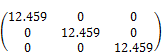
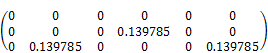
(a) Coupling matrix: represents strain charge form.
e = 
= 
(b) Elasticity matrix: represents stress charge form.
C= 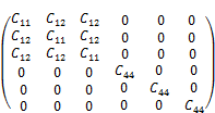
Substituting Cnm values according to table1, so, replace C11, C12, and C44 with values 1.19263E+11, 5.99859E+10 and 5.37634E+10 respectively.
The above matrices used in constitutive equations for piezoelectric effect which composed of stress charged and strain charged forms [13].
Table (1). Specifications of GaAs Substrate material.
| ε11 | 12.459 |
| ε22 | 12.459 |
| ε33 | 12.459 |
| e24 | 0.139785 |
| e32 | 0.139785 |
| e36 | 0.139785 |
| C11 | 1.19263E+11 |
| C12 | 5.99859E+10 |
| C44 | 5.37634E+10 |
3. SAW Device Model Analysis
Analysis of SAW delay line performed with COMSOL multi-physics ver. 5.0. Finite Element Method used due to its wide math equations and calculations in the field of electronic devices [14-16]. SAW delay line is modeled as a substrate layer of GaAS, Electrode layers (Au) and air gap between input and output IDTs. A 10V peak of periodic sine wave is applied to the input IDT of 4 electrodes with 1.5 GHz frequency, 2840 m/s acoustic velocity and the wavelength is 1.89 µm. A 5 cycles of output waveform is recorded as a voltage difference on fingers of IDT electrodes. Output is formed by the relation between the mechanical and electrical properties of selected piezoelectric substrate material. It is expected that the amplitude of generated waveform is less than applied input due to energy loss, interference in surface waves and with the fact of SAW decay with the thickness of substrate.
Model is built with λ/4 electrode width, four times of λ for electrode length and electrode pitch. The substrate thickness is selected λ and number of elements required for analysis (Mesh) is one tenth of λ. A time dependent analysis used with equations embedded in COMSOL
![]() (3)
(3)
![]() (4)
(4)
![]() (5)
(5)
![]() (6)
(6)
Where: ρ is the density, u is the displacement field, ![]() is the structural velocity field,
is the structural velocity field, ![]() is the relative permittivity, S is strain, E electric field, and
is the relative permittivity, S is strain, E electric field, and ![]() is remanent electric displacement.
is remanent electric displacement.
4. Simulation Results
Number of degrees of freedom solved for 56273 shown in figure (2). Complete mesh consists of 8280 domain elements, 2930 boundary elements, and 544 edge elements.
Time Dependent Solver in Solution of SAW model took Solution time of 391 s (6 minutes, 31 seconds) to perform the output. Simulation is done with 4GB RAM only and exhausted a physical memory of 773 MB and virtual memory of 840 MB. Maximum mesh size is selected as substrate thickness divided by 10. The maximum solve time step is selected as 1.3333e-11 s as a function of acoustic wave velocity and maximum mesh size. Time of displacement field is 3.32 e-9 s.
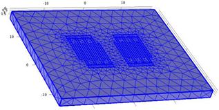
Figure (2). Physical Controlled Mesh.
Input and Output Voltages of SAW delay line IDTs have been monitored in figure (3). The output is amplified by a factor of 20 to compensate the energy loss. Comparing it with SAW delay line made of LiNaBo3 substrate, Figure (4), the output generated in a time shorter than the LiNaBo3.
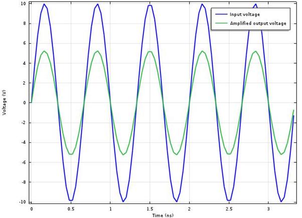
Figure (3). Applied input voltage and generated output voltage of IDTs.
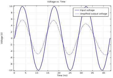
Figure (4). Input and Output Voltage recorded in SAW delay line of LiNaBo3 substrate.
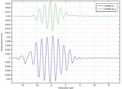
Figure (5). Displacement along X- direction.
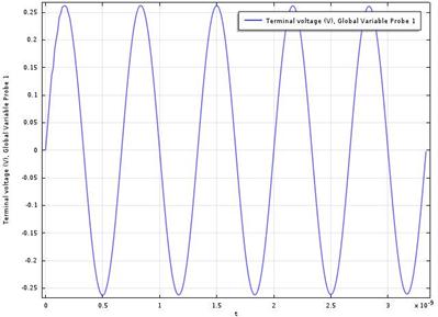
Figure (6). Rayleigh wave propagation on the surface of GaAS.
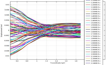
Figure (7). Elastic wave propagation along Thickness of substrate via different time periods.
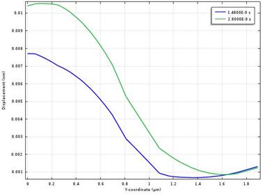
Figure (8). Displacement along thickness.
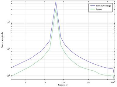
Figure (9). FFT of input voltage and output
Displacement of SAW along wave propagation (X) direction is presented and two values selected for the time, 1.68e-9 s and 6.8e-10 s with offset between them and shown in the figure (5). Rayleigh wave propagated on the surface of GaAs has been recorded in figure (6). Elastic wave propagation along Thickness of substrate, Figures (7-8) Achieves that SAW does not propagate more than the thickness of λ. Fast Fourier Transform done for the generated output signal and visualized in figure (9).
5. Conclusion
This paper introduces a simple novel method for modeling and design SAW delay line fabricated in GaAs substrate. The transient analysis of two port SAW delay line using FEM analysis in COMSOL software is presented. A time dependent study of SAW propagation on surface of piezoelectric material has been introduced using Gallium arsenide as a substrate of two port SAW delay line due to its wide applications. 3D Model for SAW device is designed as a function of the synchronous frequency and Rayleigh wavelength. The output voltage of SAW device is compared with the applied input for a 5 periodic cycles. Rayleigh wave propagation on the surface of GaAS has been visualized. Elastic wave propagation along Thickness of substrate has been monitored. Less time required to generate SAW in GaAs substrate than LiNaBo3.
References
- Macdonald, F rank Dickinson, "Experimental investigations of Mass Sensing with Surface Acoustic Devices", PhD Thesis, UC Riverside, 2010.
- Wikipedia:http://en.wikipedia.org/wiki/surface_acoustic_wave.
- Mohamed F. Elkordy, Moataz M. Elsherbini, and Aly M. Gomaa, "A comparative study of surface acoustic wave correlators ", African Journal of Engineering Research Vol. 1(2), pp. 6-16, March 2013.
- Mohamed Fahim Elkordy, Moataz Mostafa Elsherbini and Aly Mohamed Gomaa, "Modeling and simulation of unapodized surface acoustic wave filter", African Journal of Engineering Research, Volume 1, Issue 1, pp. 1-5, 2013.
- Mohamed F. Elkordy, Moataz M. Elsherbini, and Aly M. Gomaa, " A computer Simulation for The Response of an Apodized SAW Filter", journal of electrical engineering (JEE), volume 14, edition 2 , pp.213-219, Romania, 2014.
- M. M. Elsherbini, M. F. Elkordy and A. M. Gomaa, "Towards a Simple Model for SAW Delayline Using CAD", American Journal of Circuits, Systems and Signal Processing, Vol. 1, No. 3, pp.86-92, August 2015.
- M. Hofer., N. Finger, G. Kovacs, J. Schöber, U. Langer and R. Lerch (2002, October), "Finite element simulation of bulk-and surface acoustic wave (SAW) interaction in SAW devices", In Proceedings of IEEE Ultrasonics Symposium, Vol. 1, pp. 53-56, 2012.
- COMSOL, Modelling and Simulation Software: http://www.comsol.com/
- ANSYS, Simulation software:http://www.ansys.com/
- Ken-ya Hashimoto, "Introduction to Surface Acoustic Wave (SAW) Devices", http://www.te.chiba-u.jp/~ken/
- Yablonovitch, Eli; Miller, Owen D.; Kurtz, S. R, "2012 38th IEEE Photovoltaic Specialists Conference", pp. 15-56, 2012.
- Auld, Bertram Alexander, "Acoustic fields and waves in solids", Рипол Классик, 1973.
- Piezoelectric materials,http://www.efunda.com/materials/piezo/general_info/gen_info_index.cfm
- Kutiš, V., Gálik, G., Rýger, I., Paulech, J., Murín, J., Hrabovský, J., Lalinský, T. Modal and transient analysis of SAW MEMS sensor", Proc. 19th Inter. Conf. on Applied Phys. of Cond. Matter (APCOM), pp.221-224, 2013.
- Gálik, G., Kutiš, V., Murín, J., Lalinský, T., 3D FEM model of piezoelectric saw sensor. In: Proc. 20th Inter. Conf. on Applied Phys. of Cond. Matter (APCOM), pp.316-319, 2014.
- Moataz Mostafa Elsherbini, Mohamed Fahim Elkordy, Aly Mohamed Gomaa," Transient Analysis for 70MHz LiNaBo3 SAW delayline ", Journal of Scientific Research and Advances (J. Sci. Res. Adv.), Vol. 2, No. 2, pp. 80-83, June 2015.
Biography
| Moataz Mostafa Elsherbini
|
| Mohamed Fahim Elkordy
|
| Ali Mohamed Gomaa
|