
International Journal of Materials Chemistry and Physics, Vol. 1, No. 2, October 2015 Publish Date: Aug. 27, 2015 Pages: 163-173
Studies on Structural, Morphological and Optical Properties of Cobalt Doped ZnO Nanorods
Anju Singh1 *, H. L. Vishwakarma2
1Department of Physics, Rungta College of Engineering and Technology (RCET), Bhilai, Chhattisgarh, India
2Department of Physics, (VEC), Lakhanpur, Sarguja University, Ambikapur, Chhattisgarh, India
Abstract
In this paper, undoped and cobalt doped Zinc Oxide (ZnO) nanorods were achieved by a simple chemical precipitation method at room temperature in the presence of Poly Vinyl Pyrrolidone (PVP) as a capping agent. Zinc acetate (Zn (CH3COO)2.2H2O) and cobalt acetate (Co (CH3COO)2.4H2O) were taken as precursors. The effect of doping concentration ranging from 0 to 2 wt% on structural, morphological and optical properties have been studied by X-Ray Diffraction (XRD), Scanning Electron Microscopy (SEM) and Ultraviolet visible (UV-Vis) spectrophotometer. Crystallite sizes have been calculated by Debye Scherrer formula whose values are decreasing with increase in cobalt content up to 2%. The average particle size of doped nanorods is about 60 nm which is greater than that of pure ZnO (about 43 nm). It has been seen that the growth orientation of the prepared ZnO nanorods were (101). The XRD analysis also ensures that ZnO has a hexagonal (wurtzite) crystal structure. The Scanning Electron Microscope (SEM) image confirmed the size and shape of these nanorods. The absorption peaks for undoped and 1 to 2% cobalt doped ZnO nanorods samples have been observed around 355 nm, 330 nm and 380 nm by UV-Vis spectrophotometer. The doped ZnO nanorods exhibited a blue shifted band gap. The energy band gap have been obtained from the Taucs plot was found increasing up to 1% and then decreasing up to 2% of cobalt doping.
Keywords
ZnO Nanorods, Optical Band Gap, Wurtzite, XRD, SEM, Absorption Peak
Received: July 24, 2015
Accepted: August 16, 2015
Published online: August 27, 2015
@ 2015 The Authors. Published by American Institute of Science. This Open Access article is under the CC BY-NC license. http://creativecommons.org/licenses/by-nc/4.0/
1. Introduction
One dimensional semiconductor nanostructure like nanorods, nanowires, nanobelts and nanotubes has experienced more attention in recent years due to its significant properties. For future electronics, photonics [1-3] and life sciences applications [4], these materials may be used as building blocks. It has a large surface to volume ratio and direct carrier conduction path, so that it is different from the other type of nanostructure of one dimensional ZnO. It is mostly accepted that one dimensional nanostructure are useful materials for investigation of the dependence of electrical and thermal transport or mechanical properties on dimensionality and size reduction (or quantum confinement) [5]. It plays an important role both as an interconnector and of functional units in fabrication electronic, optoelectronic, electrochemical and electromechanically nanodevices [6,7].
Zinc oxide (ZnO) is a direct wide band gap semiconductor material having a band gap of 3.37eV and large excitonic binding energy 60meV at room temperature, exhibits near UV emission, transparent conductivity and piezoelectricity. One dimensional ZnO nanostructures are extensively studied for their applications in various electronic and optoelectronic devices like field effect transistors, ultra violet(UV) photo detectors, UV light emitting diodes, UV nanolaser, field emitter, solar cell etc.[8-19]. For determining the electrical and optoelectronic properties on nano devices, the surface of the nanostructure has a crucial role. As the surface to volume ratio in nanorods is very high; the surface states also play an important role on optical absorption, luminescence, photo detection and other properties. Intensive research has been focused on fabricating one dimensional ZnO nanostructures and in correlating their morphologies with their size related optical and electrical properties [20-24]. ZnO nanorods and nanowires have been widely studied because of their easy nanomaterials formation and device applications.
ZnO is an II-VI group compound semiconductor has an ionic nature is between covalent and ionic semiconductor. The crystal structure of ZnO is wurtzite, zinc blend and rocksalt, however at ambient conditions, only wurtzite phase is thermodynamically stable.
ZnO nanostructures such as nanowires, nanotubes, nanorings and nanotetrapods have been successfully grown via a variety of methods including chemical vapour deposition, thermal evaporation and electro deposition etc. ZnO nanorods with controlled shape and order could be grown by thermal vapour deposition [8,25,27], metal-organic chemical vapour deposition [28-30], molecular beam epitaxial [31], hydrothermal/solvothermal methods [32-37] and top down approach by etching [38]. Among these techniques vapour deposition and chemical methods are the widely used techniques for their versatility about controllability, repeatability, quality and mass production.
The study of effect of dopants on optical properties of ZnO based nanostructures is very important for photonic applications. Doped luminescent semiconductor nanomaterials are of great interest for possible use in optoelectronics such as light emitting diodes (LEDs) and lasers or as novel phosphors because of their interesting magnetic [39] and optical properties [40-41]. For doped nanomaterials, the method is slightly altered from that of, used for undoped semiconductor synthesis. Many semiconductors and insulators have been successfully doped with different elements such as Gd3+[42], N[43], C[44], Tb3+[45]. Compared to undoped semiconductors, doped materials offers the possibility of using the dopant to tune their electronic, magnetic and optical properties. Therefore in addition to the existing advantages, which nanomaterials have offered in terms of controllable parameters such as size, shape and surface; dopants offer the additional flexibility for designing new functionalities and for altering their properties.
Doping of transition metals has an effective method for adjusting the energy levels and surface states of ZnO. Doping various kinds of ions into ZnO is a very useful method to improve their properties. Among these ions doped ZnO, the cobalt doped ZnO has attracted much attention for its potential application in fabricating magnetic and electric devices. Cobalt is a typical element in the transition metals which has an abundant structure of electron energy state. The doped ZnO nanorods have various applications such as transparent conductors, in ferromagnetism, semiconductors and in piezoelectric and solar cells. Moreover, the nanorods have low resistivity and good optical gap energy at low temperature and transparent in the visible region.
It was observed that doping with 3d metals reduce the Eg of semiconductors by forming interband gap localized levels [46]. The charge transfer transition between the d electron of dopant and CB or VB was reported [47]. On the other hand, the metals d orbitals are mixed with the CB and VB of semiconductors [48]. This overlap is due to wide CB or VB which directly decreases Eg. Recently, there has been much attention focused on modifying ZnO by doping with transition metals such as Ag [49], Ni [50], Cu [51], Co [52], Cr [53], and Ti [54].These studies demonstrated that the metals can change Eg of ZnO and that the dopants can control ZnO grain size. ZnO: Co nanorods have been extensively studied because they exhibit high mobility, good optical transparency and good electrical conductivity and also have lower material cost.
In this present work, undoped and cobalt doped ZnO nanorods were successfully fabricated by chemical precipitation method using PVP (Poly Vinyl Pyrrolidone) as a capping agent at room temperature. The structural and morphological characterizations are carried out by XRD and SEM. The optical property is also discussed by UV-Vis absorption spectra.
2. Experimental
2.1. Materials
Cobalt doped ZnO nanorods samples were prepared by using simple chemical precipitation method. Zinc acetate dehydrate [Zn(CH3COO)2.2H2O] and Cobalt acetate tetra hydrate [Co(CH3COO)2.4H2O] were used as a starting precursors, de-ionized water as a solvent and Polyvinyl Pyrrolidone (PVP)(Mwt 4000) as a stabilized agent. Sodium hydroxide (NaOH) was also used. All the chemicals of analytical reagent grade were used from Sigma Aldrich Company which did not require any further purification. In this experimental work all the glassware used was acid washed. Ultrapure water was used for all dilution and sample preparation. Absolute ethanol was also used.
2.2. Synthesis of Co2+ Doped ZnO Nanorods
In a typical experiment 2.2gm (0.2mol/l) of Zn (CH3COO)2.2H2O in 50ml deionised water and selected precursor (cobalt acetate for Co2+) in 25ml aqueous at 1% was added drop by drop. 1gm of PVP in 50 ml deionised water was added before the precursor (doping material) for stabilizing the synthesized particles. The mixture was stirred magnetically at room temperature until a homogeneous solution was obtained. Then 0.4gm (0.2mol/l) of 50 ml sodium hydroxide was added drop by drop to the above mixture. After the NaOH injection the obtained dispersions were transparent and were purified by dialysis against deionised water and ethanol several times to remove impurities. The products were dried in hot air oven at 1000C for 1 hour.
The undoped ZnO nanorods were also synthesized by following the same procedure in the absence of the doping material.
2.3. Characterization
The morphology of the samples was characterized by the scanning electron microscopy (SEM) (JEOL-EO microscopy with accelerating voltage 20kV). The structural characterization of the samples were investigated by XPERT-PRO Diffractometer System using CuKα radiation (λ=1.54056![]() ) at 45kV and 40mA. The optical property of the sample was examined by UV-Visible spectrophotometer (Perkin Elmer λ-45) in the wavelength range of 200-800 nm.
) at 45kV and 40mA. The optical property of the sample was examined by UV-Visible spectrophotometer (Perkin Elmer λ-45) in the wavelength range of 200-800 nm.
3. Results and Discussions
3.1. Structural Study
Table 1. Effect of cobalt doping on grain size and lattice constants.
| Cobalt concentration | hkl plane | 2θ in degree | FWHM (β) in radian | d-spacing | Grain size(nm) | Lattice constants in | c/a ratio | |
| a | c | |||||||
| Undoped | 100 | 31.8384 | 0.1020 | 2.80842 | 91 | 3.2428 | 5.6167 | 1.73209 |
| 002 | 34.4937 | 0.1840 | 2.60022 | 45.23 | 2.9999 | 5.1960 | 1.73205 | |
| 101 | 36.4084 | 0.2175 | 2.46775 | 38.47 | 2.8471 | 4.9313 | 1.73205 | |
| 102 | 47.5792 | 0.3346 | 1.91120 | 25.96 | 2.2050 | 3.8191 | 1.73201 | |
| 110 | 56.6542 | 0.4488 | 1.62337 | 20.12 | 1.8744 | 3.2467 | 1.73212 | |
| 1% | 100 | 31.8309 | 0.1338 | 2.81140 | 61.76 | 3.2426 | 5.6180 | 1.73202 |
| 002 | 34.4793 | 0.1673 | 2.60127 | 49.74 | 3.0011 | 5.1981 | 1.73206 | |
| 101 | 36.3109 | 0.1171 | 2.46775 | 71.43 | 2.8545 | 4.9441 | 1.73203 | |
| 102 | 47.5864 | 0.1004 | 1.91093 | 86.51 | 2.2047 | 3.8186 | 1.73202 | |
| 110 | 56.6575 | 0.1836 | 1.62329 | 49.17 | 1.8758 | 3.2489 | 1.73200 | |
| 100 | 31.8744 | 0.2175 | 2.80766 | 38.00 | 3.2392 | 5.6105 | 1.73206 | |
| 2% | 002 | 34.4899 | 0.2509 | 2.60050 | 33.17 | 3.0002 | 5.1966 | 1.73208 |
| 101 | 36.3506 | 0.2676 | 2.47155 | 31.26 | 2.8515 | 4.9484 | 1.73536 | |
| 102 | 47.5990 | 0.1004 | 1.91045 | 86.25 | 2.2041 | 3.8176 | 1.73204 | |
| 110 | 56.6102 | 0.1428 | 1.62453 | 63.21 | 1.8758 | 3.2489 | 1.73200 | |
The crystallinity of the grown nanorods was investigated by XRD pattern. Figure 1 shows the XRD patterns of undoped and cobalt doped ZnO nanorods at different concentrations of cobalt. A definite line broadening of the XRD peaks indicates that the prepared material consists of particles in nanoscale range. From this XRD patterns analysis, we determined peak intensities, position and width and full width at half maximum (FWHM) data. The diffraction peaks at scattering angles (2θ) of 31.83840, 34.49370, 36.40840, 47.57920 and 56.65420 have been keenly indexed as hexagonal wurtzite phase of ZnO [55,56] corresponding to the reflection from (100), (002), (101), (102) and (110) crystal planes respectively are observed. The crystalline sizes of undoped and Co2+ doped ZnO nanorods were determined by means of an X-Ray line broadening method using the Scherer equation D = (kλ/β cosθ), where D is the particle size in nm, λ is the wavelength of the radiation (0.154056 nm for CuKα radiation), k is a constant equal to 0.94, β is the full width at half maximum (FWHM) intensity and θ is the peak position [57]. The estimated size of the samples from XRD patterns are of the order of 91-32 nm. The FWHM of the diffraction peaks of undoped is broader than that of the cobalt doped ZnO. This result is very much similar to reported in literature [63]. No diffraction peaks of other compounds were observed. It indicates that the ZnO nanorods prepared by chemical precipitation method have high crystallinity and high purity. It is also clear from the figure 3 that by changing the concentration of doping, the size of ZnO nanorods decreases. [64] reported that by changing the concentration of doping varying the temperature of the reaction medium, the size of the ZnO nanoparticles vary, which is due to Co ions get substituted in more number on the surface of ZnO. The crystallinity in the wurtzite structure of ZnO is restored by addition of cobalt as a dopant which is confirmed by increase in the intensity of the main peak (101) as the concentration of cobalt increased from 1% to 2%. No extra peaks were found in the patterns that shows the formation of the single phase. This indicates that the doped Co atoms substitute Zn atoms without changing ZnO wurtzite structure. The lattice parameters calculated from XRD data demonstrate that their values are close to but slightly greater than those of pure ZnO (see table1). The lattice parameters decrease when the concentration of the doping increases (figure 2). Although the change is very small, the concentration of the doping plays an important role in the variation of lattice parameters. This gives an indication for the Co substitution in the ZnO crystalline structure since the ionic radii of Co2+ (0.058nm) is less than that of Zn2+ (0.060nm) [58].
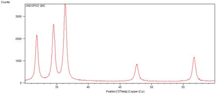
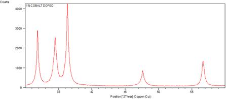
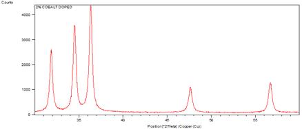
Figure 1. XRD patterns of undoped and cobalt doped ZnO nanorods.
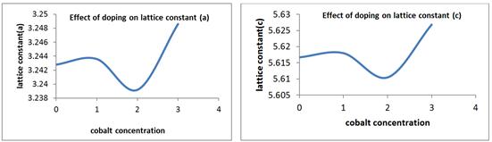
Figure 2. Effect of doping on lattice constants (a) and (c).

Figure 3. Effect of doping on grain size of ZnO nanorods.

Figure 4. FWHM curve of ZnO nanorods at different concentration of cobalt.
It can be observed that from the figure 1, the crystal structure remains hexagonal even with maximum doping; that is at 2% Co doped ZnO. However an inclination from (002) to (101) orientation has been observed with increase (at 1% to 2%) in Co doping percentage. This may be due to the fact that, in addition to substitutional sites, Co may also start to occupy interstitial sites due to the deformation of lattice structure caused by substitution of nearby Zn atoms by other Co atoms. This will also result in an increase of lattice constant.
The FWHM curve in figure 4 indicates the growth of nanorods along a preferred direction.
3.2. Morphological Study
The morphology of the products was analyzed with the scanning electron microscopy (SEM). The SEM morphologies of undoped and 1-2% cobalt doped ZnO nanorods as synthesized are shown in figure 5. The SEM image clearly shows that at low magnification the size of undoped ZnO is 10µm and their shape is in rod form. But Co doped ZnO shows the formation of many spherical particles at low and high magnification. At high magnification the size of undoped ZnO nanorods is in the range of 5-1µm (see figure 6 and 7). It is clear from the observation that there is no change in the size of the particles at low and high magnification but their shapes are changed. It is interesting to note that the grain size observed from SEM is different from the grain size determined by using XRD.
3.3. Optical Properties
UV-Visible absorption spectroscopy is a powerful technique to explore the optical properties of semiconducting nanoparticles. The absorbance is expected to depend on several factors like band gap, oxygen deficiency, surface roughness and impurity centres [59]. The optical properties of undoped and different concentration of cobalt doped ZnO nanorods were studied by UV-Vis absorption spectroscopy. The absorption spectra of undoped and cobalt doped ZnO nanorods with different concentrations have been seen in figure 8.
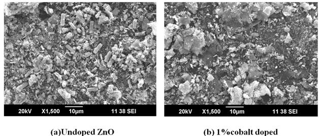

Figure 5. SEM image of undoped and cobalt doped ZnO nanorods at low magnification.
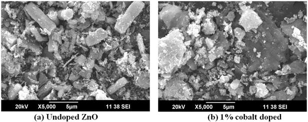

Figure 6. SEM image of undoped and cobalt doped ZnO nanorods at high magnification.
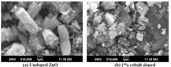

Figure 7. SEM image of undoped and cobalt doped ZnO nanorods at very high magnification.
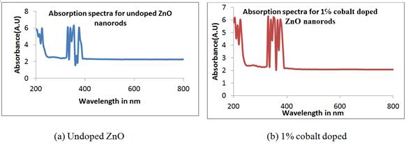

Figure 8. UV-VIS absorption spectra of undoped and cobalt doped ZnO nanorods at different concentrations.
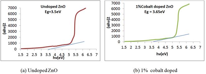

Figure 9. Taucs plot of ZnO nanorods at different concentration of cobalt.
The absorption peak for undoped ZnO nanorods can be observed around 355 nm. For 1% and 2% cobalt doped ZnO samples exhibit the absorption peak at 330 nm and 380 nm. The sharp edge of the samples indicates high crystal quality. These absorption peaks are blue shifted. [64] reported that the position of the absorption spectra is shift towards the lower wavelength side with increasing cobalt doping concentration in ZnO. A blue shift of the absorption edges with increasing doping concentration indicates an increase in the band gap of the system. This is because the addition of cobalt ions into Zn sites affects the electronic band structure of the material. The optical band gap of the nanorods was determined by applying the Tauc relationship [60] as given below
![]()
where α is the absorption coefficient (α = 2.303A/t), here A is the absorbance and t is the thickness of the cuvett, B is a constant , h is plank constant , ν is the photon frequency and Eg is the optical band gap. The value of n = 1/2, 3/2, 2 or 3 depending on the nature of the electronic transition responsible for absorption and n = 1/2 for direct band gap semiconductor. An extrapolation of the linear region of a plot of (αhν)2 on the Y-axis versus photon energy (hν) on the X-axis gives the value of the optical band gap as shown in figure 9. The calculated band gap of nano powder of ZnO was found to be 3.50 eV while it is 3.37 eV in case of bulk ZnO. These figures show a large blue shift of the band gap corresponding to the samples of undoped and 2% cobalt doped ZnO nanorods. It is evident from the graphs that the direct band gap increases for 1% cobalt doping whereas it decreases for 2% cobalt content. This is in good agreement with the quantum confinement effects of nanoparticles [61].
The optical absorption spectra and the calculated band gap are relatively higher as compared to their bulk counterparts. They exhibit a blue shift in the absorption band edge which could be attributed to well known quantum size effect of semiconductor, indicating that the band gap increases as the particle approaches to nano regime. Therefore the increases in band gap in the present study can also be explained on the basis of decrease in the lattice parameters for the cobalt content, which is due to the smaller size of Co2+ (ionic radii ~72![]() ) as compared to Zn2+ (ionic radii~74
) as compared to Zn2+ (ionic radii~74![]() ). The increase in the band gap can also be studied on the basis of Moss - Burstein effect [62]. When Fermi level shifts close to the conduction band due to increase in carrier concentration, the lower energy transitions are blocked and the value of the band gap increases for doping 1%. Further the decrease in the band gap when concentration level increases to 2% may be due to the formation of new orbital of cobalt mixed and to the transitions between partially forbidden valance bands to conduction band.
). The increase in the band gap can also be studied on the basis of Moss - Burstein effect [62]. When Fermi level shifts close to the conduction band due to increase in carrier concentration, the lower energy transitions are blocked and the value of the band gap increases for doping 1%. Further the decrease in the band gap when concentration level increases to 2% may be due to the formation of new orbital of cobalt mixed and to the transitions between partially forbidden valance bands to conduction band.
Generally an excess carrier through doping denoted imputes lead to the blue shift of optical band to band transitions of the cobalt doped ZnO nanorods. This is the phenomenon that the fermi levels merges into the conduction band with an increase in the carrier concentration. The low energy transitions are not allowed. It is indicated that lattice distortion may arise due to more Co doped in ZnO host.
4. Conclusions
In this study, the structural, morphological and optical properties of undoped and cobalt doped ZnO nanorods have been synthesized by simple chemical precipitation method with different concentrations of cobalt. The structural characterization of the nanorods showed wurtzite structure with the (101) plane as the predominant orientation. The average particle size of doped nanorods is about 60 nm which is greater than that of pure ZnO (about 43 nm). Simple chemical precipitation grown cobalt doped ZnO showed good crystallinity suggesting the substitution of Zn ion by Co ion as evident from XRD and UV-Vis spectrum. XRD results showed that the Co ions replaced by Zn ions without changing the wurtzite structure, whose lattice parameters are also similar to that of ZnO. The lattice parameter decreases by increasing doping concentration. The absorption peak for undoped, 1% and 2% cobalt doped ZnO nanorods samples have been observed around 355 nm, 330 nm and 380 nm. Energy band gap varies from 3.5 eV to 3.65 eV with 1% cobalt doping and all values are higher as compared to bulk (3.37 eV). This unique property of cobalt doped ZnO can be used to fabricate transparent electrodes in flat panel displays and metal insulator semiconductor diodes.
Acknowledgement
Authors are thankful to SAIF Kochi, Ernakulum for characterization of samples by SEM technique, SAIF Punjab University, Chandigarh for XRD studies. We are also thankful to RDVV University for providing UV-Visible absorption spectra.
References
- D.Appell,Nanotschnology: wired for success, Nature.,419 553 (2002).
- L.Samuelson, Self-forming nanoscale devices, Mater. Today, 6, 22 (2003).
- X FDuan, Y Huang, J F Wang and C MLieber,Indium phosphide nanowires as building blocks for nanoscale electronic and optoelectronic devices, Nature.,409 ,66 (2001).
- Y Cui, Q Wei, H Park and C M Lieber,Nanowire nanosensors for highly sensitive and selective detection of biological and chemical species, Science., 293,1289 (2001).
- Y N Xia, P D Yang, Y G Sun, Y YWu, B Mayers, B Gates, Y D Yin, F Kim and H Q Yan, One-dimensional nanostructures: synthesis, characterization and applications, Adv.Mater.,15, 353 (2003).
- Z LWang, Characterizing the structure and properties of individual wire-like nanoentities, Adv. Mater., 12, 1295 (2000).
- J Hu, T W Odom and C MLieber, Chemistry and physics in one dimension: synthesis and properties of nanowires and nanotubes, Acc.Chem.Res., 32, 435 (1999).
- M. H. Huang, Y. Wu, H. Feick, N. Tran, E.Weber and P. Yang 13, Catalytic growth of Zinc Oxidenanowires by vapor transport, Adv. Mater. b, Vol.13, pp. 113-116 (2001).
- Z.-M Liao, K.-J Liu, J.-M Zhang, J. Xu, and D.-P Yu, Effect of surface states on electron transport in individual ZnO nanowires, Phys. Lett. A., Vol.367, pp. 207-210 (2007).
- Q. H. Li, T.Gao, Y. G. Wang and T. H. Wang, Adsorption and desorption of oxygen probed from ZnO nanowire films by photocurrent measurements, Appl. Phys. Lett..,Vol.86, pp. 123117 (2005).
- H. Kind, H. Q. Yan, B.Messer, M.Law andP. D. Yang, Nanowire ultravioletphotodetectors and optical switche, Adv. Mater., Vol.14, pp. 158–160 (2002).
- C. Soci, A.Zhang, B. Xiang, S. A. Dayeh, D. P. R.Aplin, J.Park, X. Y.Bao, Y. H. Lo,and D.Wang, ZnO nanowire UV photodetectors with high internal gain, NanoLett. , Vol.7, pp. 1003-1009 (2007).
- N. H. Alvi, M. Riaz, G.Tzamalis,O.Nur and M.Willander, Fabrication andcharacterization of high-brightness light emitting diodes based on n-ZnOnanorodsgrown by a low-temperature chemical method on p-4H-SiC and p-GaN, Semicond.Sci. Technol., Vol.25, pp. 065004 (2010).
- J.Liu, Y. H. Ahn, J.-Y Park,K. H. Koh and S. Lee, ,Hybrid light-emitting diodes based on flexible sheets of mass-produced ZnO nanowires, Nanotechnol.,Vol.20, pp.4452063 (2009).
- M. Law, L. E. Green, J. C. Jhonson, R.Saykally andP.Yang, Nanowire dye-sensitized solar cells, Nature Mater., Vol.4, pp. 455-495 (2005).
- M. Law, L. E. Greene, A.Radenovic, T.Kuykendall, J.Liphardt and P.Yang, ZnOAl2O3 and ZnO-TiO2 core-shell nanowire dye-sensitized solar cells, J. Phys. Chem. B.,Vol.110, pp. 22652-22663 (2006).
- K. S Yeong, M. K H.and J. T. L Thong, The effects of gas exposure and UVillumination on field emission from individual ZnO nanowires, Nanotechnol., Vol.18, pp. 185608 (2007).
- S.Xu, Y.Qin, C.Xu, Y.Wei, R.Yang and Z. L Wang, Self-powered nanowire devices, Nat. Nanotechnol., Vol.5, pp. 366-373 (2010).
- D. J Gargas, M. Eugenia, T. Molares and P Yang, Imaging single ZnO vertical nanowire laser cavities using UV-laser scanning confocal microscopy, J. Am. Chem.Soc.,Vol.131, No.6, pp. 2125-2127 (2009). doi:10.1021/ja8092339.
- K Keem, H Kim, G T Kim, J S Lee, B Min, K Cho, M Y Sung and S Kim, Photocurrent in ZnO nanowires grown from Au electrodes, Appl.Phys.Lett., 84, 4376 (2004).
- M S Arnold, PAvouris, Z W Pan and Z L Wang , Field effect transistors based on single semiconducting oxide nanobelts, J.Phys.Chem.B.,107, 659 (2003).
- M H Huang, S Mao, H Feick, H Q Yan, Y Y Wu, H Kind, E Weber, R Russo and P D Yang, Room temperature ultraviolet nanowire, nanolasers Science.,292, 1897 (2001).
- C J Lee, T J Lee, S C Lyu, Y Zhang, H Ruh and H J Lee, Field emission from well aligned zinc oxide nanowires grown at low temperature, Appl. Phys.Lett., 81, 3648 (2002).
- W I Park, Y H Jun, S W Jung and G C Yi,Excitonic emission observed in ZnOsingle crystal nanorods, Appl.Phys.Lett.,82,964 (2003).
- P. K. Giri, S. Dhara and R. Chakra borty, Effect of ZnO seed layer on the catalytic growth of vertically aligned ZnOnanorod arrays, Mater. Chem. Phys.,Vol.122, pp. 18-22 (2010).
- C.Li,G.Fang, J. Li, L.Ai, B.Dong andX.Zhao, Effect of seed layer on structural properties of ZnOnanorod arrays grown by vapor-phase transport, J. Phys. Chem. C., Vol.112, pp. 990-995 (2008).
- B. D. Yao, Y. F. Chan and N.Wang, Formation of ZnO nanostructures by a simple way of thermal evaporation, Appl. Phys. Lett.,Vol.81, pp. 757-759 (2002).
- H. Yuan and Y.Zhang, Preparation of well-aligned ZnO whiskers on glass substrate by atmospheric MOCVD, J. Cryst. Growth, Vol.263, pp. 119–124 (2004).
- W. I. Park, D. H.Kim, S. W. Jung and G. C. Yi,Metalorganicvapor-phase epitaxial growth of vertically well-aligned ZnOnanorods, Appl. Phys. Lett., Vol.80, pp. 4232–4234 (2002).
- D. C. Kim, B. H. Kong, and H. K Cho, Synthesis and growth mechanism of catalyst free ZnOnanorods with enhanced aspect ratio by high flow additional carrier gas at low temperature, J. Phys. D: Appl. Phys.,Vol.42, pp. 065406 (2009).
- Y. WHeo, V.Varadarajan, M.Kaufman, K.Kim, D. P. Norton, F.Ren, andP. H. Fleming, Site-specific growth of ZnOnanorods using catalysis-driven molecular-beam epitaxy, Appl. Phys. Lett., Vol.81, pp. 3046–3048 (2002).
- M.Breedon, C.Rix and K.Kalantar-zadeh,Seeded growth of ZnOnanorods from NaOH solutions, Mater. Lett., Vol.63, pp. 249–251 (2009).
- M. A. Verges, A. Mifsud and C. J. Serna, Formation of rodlike zinc-oxide microcrystals in homogeneous solutions, J. Chem. Soc., Faraday Trans., Vol.86, pp. 959-963 (1990).
- N. H. Alvi, M. Riaz, G.Tzamalis, O.Nur and M.Willander, Fabrication and characterization of high-brightness light emitting diodes based on n-ZnOnanorods grown by a low-temperature chemical method on p-4H-SiC and p-GaN, Semicond. Sci. Technol., Vol.25, pp. 065004 (2010).
- Y.Tak andK.Yong Controlled growth of well-aligned ZnOnanorod array using a novel solution method, J. Phys. Chem. B, Vol.109, pp. 19263-19269 (2005).
- C.Pacholski, A.Kornowski and H. Weller, Self-assembly ofZnO: from nanodots to nanorods, Angew. Chem. Int. Ed.,Vol.41, pp. 1188-1191 (2002).
- J. Songand S.Lim, Effect of seedlayer on the growth of ZnOnanorods, J. Phys. Chem. C,Vol.111, pp. 596-600 (2007).
- J. J. Wu, H. I. Wen, C. H. Tseng and S. C. Liu, Well-aligned ZnOnanorods via hydrogen treatment of ZnO films, Adv. Funct. Mater. Lett., Vol.14, pp. 806–810 (2004).
- X. Huang, G. Li, B. Cao, M. Wang and C. Hao, J.Phys. Chem. C, 113, 4381 (2009).
- G. Murugadoss,J. Lumin., 132, 2043 (2012).
- K.M.K. Srivatsa, D. Chhikara and M. Senthil Kumar, .J. Mater. Sci. Technol., 27, 701 (2011).
- W.Y. Zhou, Y. Zhou and S.Q. Tang, Mater. Lett., 59, 3115 (2005).
- H. Tokudome and M. Miyauchi, Chem. Lett., 33, 1108 (2004).
- J.H. Park, S. Kim and A.J. Bard, Nano Lett., 6, 24 (2006).
- M.G. Ou, B. Mutelet, M. Martini, R. Bazzi, S. Roux,G. Ledoux, O. Tillement and P. Perriat, J. ColloidInterf. Sci. 333, 684, (2009).
- G.Campet, M.Jakani, J. P. Doumerc, J.Claverie, P. Hagenmuller, Photoconduction mechanisms in titanium and rare earth n-typesemiconducting electrodes with pyrochlore and perovskite structures, Solid State Communications, 42(2), 93-6 (1982).
- W.Choi, A. Termin, M. Hoffmann, The role of metal ion dopants in quantum-sized TiO2: correlation between photoreactivity and charge carrier recombination dynamics,The Journal of Physical Chemistry, 98(51), 13669-79 (1994).
- T.Umebayashi, T.Yamaki, H.Itoh, K. Asai,Analysis of electronic structures of 3d transition metal-doped TiO2 based on band calculations, Journal of Physics and Chemistry of Solids,63(10), 1909-20 (2002).
- R.Wang,J. H. Xin, Y. Yang,H.Liu, L. Xu, J. Hu, The characteristics and photocatalytic activities of silver doped ZnOnanocrystallites, Applied Surface Science,227(1-4), 312-7 (2004).
- C. J. Cong,J. H. Hong, Q. Y.Liu, L.Liao, K. L. Zhang, Synthesis, structure and ferromagnetic properties of Ni-doped ZnO nanoparticles, Solid State Communications,138(10-11), 511-5 (2006).
- K. G. Kanade, B. B Kale, J.-O. Baeg,S. M. Lee, C. W Lee, S.-J Moon, H. Chang,Self-assembled aligned Cu doped ZnO nanoparticles for photocatalytic hydrogen production under visible light irradiation, Materials Chemistry and Physics ,102(1), 98-104 (2007).
- N. Volbers, H.Zhou, C.Knies, D. Pfisterer, J. Sann, D. M.Hofmann, B. K. Meyer, Synthesis and characterization of ZnO:Co<sup>2+</sup> nanoparticles, Applied Physics A: Materials Science & Processing.,88(1), 153-5 (2007).
- L .Li, W. Wang, H. Liu, X. Liu, Q .Song andS.Ren, First principles calculations of electronic band structure and optical properties of Cr-doped ZnO, The Journal ofPhysical Chemistry C ,113(19), 8460-4 (2009).
- N. Samaele, P.Amornpitoksuk andS.Suwanboon, Morphology and optical properties of ZnO particles modified by diblock copolymer, Materials Letters, 64(4), 500-2 (2010).
- J. Zhou, F. Zhao, Y. Wang, Y. Zhang, and L. Yang, Size-controlled synthesis of ZnO nanoparticles and their photoluminescence properties,Journal of Luminescence, vol. 122-123, no. 1-2, pp. 195–197 (2007).
- Z. M. Khoshhesab, M. Sarfaraz, and M. A. Asadabad,Preparation of ZnO nanostructures by chemical precipitation method, Synthesis and Reactivity in Inorganic,Metal-Organic and Nano-Metal Chemistry,vol. 41, no. 7, pp. 814–819 (2011).
- X.H. Huang, Z.Y. Zhan, X. Wang, Z. Zhang, G.Z.Xing, D.L. Guo, D.P. Leusink, L.X. Zheng and T. Wu, Appl. Phys. Lett., 97, 203112 (2010).
- R.D. Shannon, ActaCrystallogr. Sect. A,32 (Sep1) 751–767 (1976).
- A.S. Ahmed, M.M. Shafeeq, M.L. Singla, S. Tabassum, A.H. Naqvi, A. Azam,J.Lumin., 1,131 (2010).
- J. Tauc, Amorphous and Liquid Semiconductors, Plenum Press, New York, p. 171 (1974).
- T. Takagahara, K. Takeda,Phys. Rev. B, 46, 15578(1992).
- S. Suwanboon, T. Ratana, W.T. Ratana, Walailak, J. Sci. Technol.,4 (1),111(2007).
- G. Murugadoss,Synthesis and Characterization of Transition Metals Doped ZnONanorods, J. Mater. Sci. Technol., 28(7), 587-593(2012).
- S. Udayakumar, V.Renuka and K.Kavitha,Structural, optical and thermal studies of cobalt doped hexagonal ZnO by simple chemical precipitation method,J. Chem. Pharm. Res.,4(2),1271-1280 (2012).


