
International Journal of Materials Chemistry and Physics, Vol. 1, No. 1, August 2015 Publish Date: Jul. 23, 2015 Pages: 86-92
Effect of Surfactant on Electrical Characterization of ZnO Thin Film Based MOS Capacitors
M. Vishwas1, *, K. Narasimha Rao2, Ashok M. Raichur3
1Department of Physics, Government Science College (Autonomous), Bangalore, India
2Department of Instrumentation and Applied Physics, Indian Institute of Science, Bangalore, India
3Department of Materials Engineering, Indian Institute of Science, Bangalore, India
Abstract
Zinc oxide (ZnO) thin films were prepared on p-silicon (100) substrates by the sol-gel technique using zinc acetate dehydrate as a precursor material with and without surfactant. The films were heat treated by microwave-assisted method and annealed at various temperatures in ambient air. Different nano-structures were obtained by the varying annealing conditions. The structural characterization of ZnO films were carried out using x-ray diffraction (XRD) and scanning electron microscopy (SEM). The metal-oxide-semiconductor (MOS) capacitors were fabricated using ZnO film. The electrical properties of ZnO films with surfactant were studied from current-voltage (I-V), dissipation-voltage (D-V) and capacitance-voltage (C-V) characteristics and found that the dielectric constant of ZnO film increased with the additive surfactant. The leakage current density in ZnO film decreased and resistivity increased with surfactant.
Keywords
ZnO, Sol-Gel, Thin Films, Nano-Structures, MOS-Capacitor
Received: June 27, 2015
Accepted: July 4, 2015
Published online: July 22, 2015
@ 2015 The Authors. Published by American Institute of Science. This Open Access article is under the CC BY-NC license. http://creativecommons.org/licenses/by-nc/4.0/
1. Introduction
ZnO is an important II-VI group semiconducting metal oxide nano-material with a wide band gap of 3.3 eV, which has received a great deal of attention because of its use in various domains. ZnO is used in various optics and opto-electronic applications because of its high dielectric constant, large band gap energy and high optical transparency. ZnO is used as room temperature and high temperature luminescence material, nanolaser, light emitting diode (LED), and dye sensitized solar cell because of high exiton binding energy (~60 meV). ZnO can be used in the field of sensors and actuators as a piezoelectric material for UV and gas sensing. ZnO is used in nano-piezotronics as piezoelectric field effect transistor, piezoelectric diode etc. [1]. ZnO is also used for the production of energy that is by photo-catalysis, for producing H2 from H2O. ZnO is used in biomedical applications as a biocompatible, biodegradable and non-toxic material [1]. ZnO nano-films/ particles are used as photo-catalyst (as a substitute to TiO2) for the degradation of toxic organic dyes/compounds [2,3]. ZnO film can also be used as channel layer between source and drain in thin film transistors (FETs) [4]. ZnO films can be synthesized by various physical and chemical methods [5], of which the sol-gel method [6] is preferred because of the possibilities of uniform deposition on large substrates at room temperature and cost effectiveness. ZnO exhibits various nanostructures including nano-rods [7], nano-wires [8],nano-tubes [9] and nano-needles [10]. Kajbafvala et al. [11] reported the microwave assisted synthesis of sword-like ZnO nano-wires. Qurash et al. [12] reported the ultra-fast and large-quantity synthesis of one-dimensional ZnO nano-wires by microwave-assisted method. Ali Eftekhari et al. [13] reported the synthesis and characterization of flower like bundles of ZnO nano-sheets by hydrothermal method.
In this paper, the synthesis, structural and electrical characterization of ZnO nanostructures prepared by the sol-gel method and microwave irradiation PEG additive ZnO films have been reported.
2. Experimental Work
Zinc acetate dihydrate was used as the precursor material of ZnO. Isopropyl alcohol and diethanolamine (DEA) were used as a solvent and stabilizer, respectively. Zinc acetate dihydrate (molecular weight:219.50) was dissolved in isopropyl alcohol under constant stirring using a magnetic stirrer and DEA was added drop wise for complete dissolution of precursor and to get the transparent sol of ZnO at room temperature. The concentration of zinc acetate was 0.5 M and the molar ratio of diethanolamine to zinc acetate was tuned to 1:1. The resultant ZnO sol was stirred for 2 h to get a clear and homogeneous solution, which was stored in an air tight beaker as a stock solution. After 4 h, a few drops of the sol were placed on p-silicon (100) substrates and spin coated for 30 sec at 3000 rpm. Prior to film deposition, the silicon substrates were cleaned with RCA-1 and RCA-2 solutions. The details of cleaning procedure are given in our previous paper [14]. ZnO sol was mixed with 3 wt. percent polyethylene glycol (PEG) (molecular weight: 600) and spin coated on silicon substrates in the same way. As prepared ZnO and PEG additive ZnO films were dried in a hot air oven at 60oC for 15 min and then annealed at constant temperature from 400 - 800oC for 1 h in air. ZnO films were also heat treated by microwave irradiation at different powers (480 W & 640 W) for 5 min. The MOS capacitors were fabricated using PEG additive ZnO films. The details of fabrication of MOS capacitors are given previously [14]. The area of the electrode was 0.554 x 10⁻⁶ m2.The XRD spectra were obtained by using Philips diffractometer with monochromatic Cu-Kα radiation. The film thickness was measured by stylus method using Dektak profiler (DEKTAK 3). The film morphology was studied using scanning electron microscopy (SEM) (Raith, eLiNE). The C–V, I–V and D–V measurements were taken using Agilent 4155C & 4284 LCR meter.
3. Results and Discussions
Fig. 1 shows the XRD patterns of ZnO films prepared without surfactant annealed at temperatures of 400, 500, 700 and 800oC for 1 h in ambient air. It was observed, the ZnO film exhibited polycrystalline wurtzite structure after annealing at 400oC. The intensity of the peaks increased with increasing annealing temperature, indicating the improvement in crystallinity of the film. The intensity of (100) peak enhanced after annealing at 800oC, which depicts the preferential growth of grains parallel to a-axis. XRD patterns of microwave irradiated ZnO films are shown in Fig. 2.
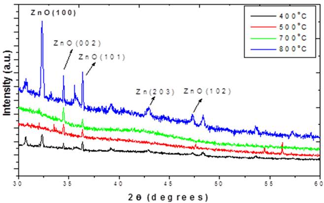
Fig. 1. XRD patterns of ZnO films without PEG annealed at different temperatures in air.
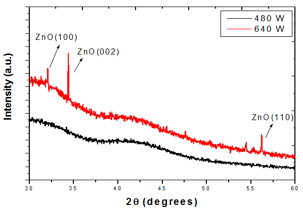
Fig. 2. XRD patterns of ZnO films without PEG microwave irradiated at (a) 480 W (b) 640 W.
It was observed, the film irradiated at a power of 480 W for 5 min was amorphous, whereas the film irradiated at 640 W was crystalline in nature as indicated by the diffraction peaks (100) and (002). The crystallinity of the thermally annealed ZnO films was greater than microwave irradiated films.
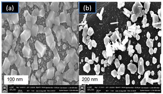
Fig. 3. SEM images of ZnO films without PEG annealed at (a) 700oC and (b) 800oC in air.
Fig. 3 shows the SEM images of the ZnO films synthesized without surfactant annealed at 700oC and 800oC for 1h. It is clear from the figures that the morphology of ZnO film changed with annealing temperature from rod like structure to four different nano-structures, including spherical, pentagonal, hexagonal and nano-rods after annealing at 800oC for 1 h. The average size of the rod is 100 nm width and 300 nm length after annealing at 700oC where as for the film annealed at 800oC, the width and length of nano-rods were ~ 80 nm and 600 nm, respectively. ZnO film annealed at 400 and 500oC for 1 h exhibited granular structures and irregular and spherical nanostructures, respectively [15].
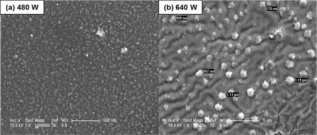
Fig. 4. SEM images of ZnO films without PEG microwave irradiated at (a) 480 W (b) 640 W.
Fig. 4 shows the SEM images of microwave irradiated ZnO film synthesized without surfactant at 480 W and 640 W for 5 min. It depicts that the film irradiated at 480 W is amorphous as the grains are not formed and the film is featureless while, the film irradiated at 640 W is in crystalline phase as indicated by the nano-stars formed on the surface of the film. The average size of the stars was ~ 900 nm.
The crystal structure of the 3wt.% PEG additive ZnO film annealed at 500oC for 1 h is shown by XRD patterns in Fig. 5. It was observed from the figure that the PEG additive ZnO film exhibited hexagonal wurtzite phase with preferred orientation along c-axis perpendicular to the substrate indicated by the predominant peak of (002) plane.
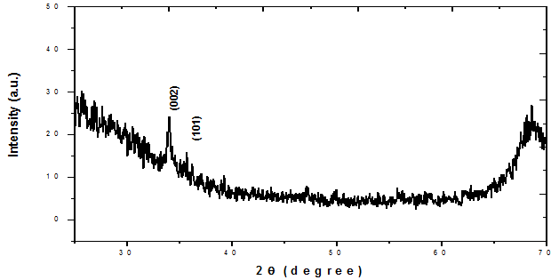
Fig. 5. XRD pattern of 3% PEG additive ZnO film annealed at 500oC for 1 h in air.
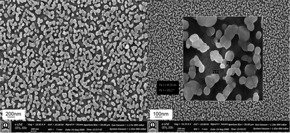
Fig. 6. SEM images of 3wt.% PEG additive ZnO film annealed at 500oC for 1 h in air.
Fig. 6 shows the SEM images of 3wt. % PEG additive ZnO film annealed at 500oC for 1 h in air. It is clear from the figure the grains of ~ 45 nm were separated with one another with a larger distance between them, so that the porosity of the ZnO film increased with the addition of PEG. Also, the surface area of the ZnO film increased with the addition of PEG. Hence, ZnO-PEG film become more porous as compared to ZnO:Al [16], ZnO:Sn [17] and ZnO film [15].
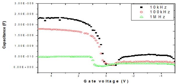
Fig. 7. Capacitance versus voltage plot of 3wt.% PEG additive ZnO film annealed at 500oC for 1 h in air.
The capacitance-voltage characteristics of 3 wt. % PEG additive ZnO film deposited on silicon substrate annealed at 500oC for 1 h is shown in Fig. 7. The film thickness was 105 nm. The values of oxide capacitance at 10 kHz, 100 kHz and 1 MHz were 2.32 nF, 1.78 nF and 0.502 nF, respectively. The corresponding dielectric constants were determined to be 49.6, 38.1 and 10.7, respectively. The dissipation-voltage characteristics of 3 wt. % PEG additive ZnO film annealed at 500oC is shown in Fig. 8. The dissipation at 5V was ~1.0 measured at 1MHz.
The I-V characteristics of PEG additive ZnO film is shown in Fig. 9. It is evident from Fig. 9 that the forward current remain almost constant with increase in the gate voltage up to 4 volts and after the current increased with gate voltage non-linearly which exhibits rectifying character. The resistivity and leakage current density were calculated at the gate voltage of 5 V and were found to be 5.38x10⁸ Wcm and 0.88 x 10⁻³ A/cm2, respectively. While, the ZnO film synthesized without PEG exhibited an electrical resistivity of 4.224 x 10⁷ Wcm and a leakage current density of 1.27 x 10⁻² A/cm2 after annealed at 500oC for 1 h in air [15]. Hence the addition of PEG decreased the leakage current density and increased the resistivity of the ZnO film.
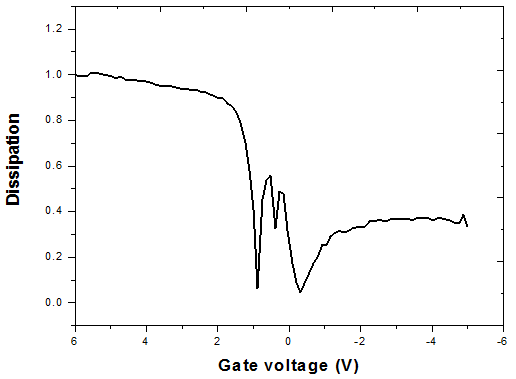
Fig. 8. Dissipation versus voltage plot of 3 wt.% PEG additive ZnO film annealed at 500oC (measured at 1 MHz).
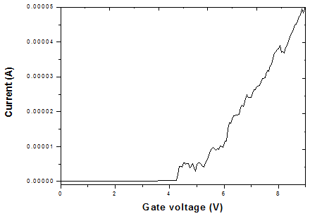
Fig. 9. I-V characteristics of 3wt% PEG additive ZnO film annealed at 500oC for 1 h in air.
4. Conclusions
In summary, the ZnO thin films with and without surfactant were successfully synthesized by the sol-gel route. The effect of surfactant on electrical characterization of MOS capacitors was investigated. The ZnO films with surfactant showed high resistivity and low leakage current density. These films are suitable for the fabrication of CMOS devices.
Acknowledgements
The authors are thankful to the Indian Nanoelectronics Users Programme (INUP), Centre for Nanoscience and Engineering (CeNSE), Indian Institute of Science (IISc), Bangalore, funded by the Department of Information Technology (DIT), Government of India for partial support of this work.
References
- Wang, Z. L., (2009),ZnO nanowire and nanobelt platform for nanotechnology.Mat. Sci. & Eng. R,64,33–71.
- Pal, B., and Sharon, M., (2002), Enhanced photocatalytic activity of highly porous ZnO thin film prepared by Sol-Gel process. Mat. Chem. & Phys., 76, 82-87.
- Kaneva, N., Stambolova, I., Blaskov, V., Dimitriev, Y., Vassilev, S.and Dushkin, C., (2010), Photocatalytic activity of nanostructured ZnO films prepared by two different methods for the photoinitiated decolorization of malachite green. J. Alloys & Comp., 500, 252-258.
- Hoffman, R. L., Norris, B. J., Wager,J. F., (2003),ZnO-based transparent thin-film transistors. Appl. Phy. Lett.,82, 733-735.
- Xu, S. and Wang, Z. L., (2011),One-Dimensional ZnO Nanostructures: Solution Growth and Functional Properties.Nano Res.,4(11), 1013-1098.
- Vishwas, M., Narasimha Rao, K., Arjuna Gowda, K.V. and Chakradhar,R.P.S.,(2010),Effect of sintering on optical, structural and photoluminescence properties of ZnO thin films prepared by sol–gel process.Spectrochimica Acta Part A, 77, 330-333.
- Park, W.I., Jun, Y.H., Jung, S.W. and Yi, G.C., (2003), Excitonic emissions observed in ZnO single crystal nanorods. Appl. Phys. Lett., 82, 964-966.
- Kong, Y.C., Yu, D.P., Zhang, B., Fang, W. and Feng, S.Q., (2001), Ultraviolet-emitting ZnO nanowires synthesized by a physical vapor deposition approach.Appl. Phys. Lett.,78, 407-409.
- Hu, J.Q. and Bando, Y., (2003),Growth and optical properties of single-crystal tubular ZnO whiskers.Appl.Phys. Lett.,82, 1401-1403.
- Yuvaraj, D. and Narasimha Rao, K. (2009), Selective growth of ZnO nanoneedles by thermal oxidation of Zn microstructures. Mat. Sci. Engg. B, 164, 195-199.
- Kajbafvala, A., Shayegh, M. R., Mazloumi, M., Zanganeh, S., Lak, A., Mohajerani, M. S. and Sadrnezhaad, S.K., (2009), Nanostructure sword-like ZnO wires: rapid synthesis and characterization through a microwave-assisted route. J. Alloys & Compounds, 469, 293-297.
- Qurashi, A., Tabet, N., Faiz, M. and Yamzaki, T. (2009), Ultra-fast microwave synthesis of ZnO nanowires and their dynamic response toward hydrogen gas. Nanoscale Res. Lett., 4, 948-954.
- Eftekhari, A., Molaei, F. and Arami, H. (2006),Flower-like bundles of ZnO nanosheets as an intermediate between hollow nanosphere and nanoparticles.Mat. Sci. Engg. A,437, 446-450.
- Vishwas, M., Narasimha Rao, K., Phani, A.R., Arjuna Gowda, K.V. and Chakradhar,R.P.S., (2011),Spectroscopic and electrical properties of SiO2 films prepared by simple and cost effective sol-gel process.Spectrochimica Acta Part A,78, 695-699.
- Vishwas, M., Narasimha Rao, K., Phani, A.R., Arjuna Gowda, K.V. and Chakradhar,R.P.S., (2011),Effect of Annealing Temperature on Electrical and Nano-structural properties of sol-gel derived ZnO Thin Films.J Mater Sci: Mater Electron.,22, 1415-1419.
- Vishwas, M., Narasimha Rao, K., Phani, A.R., Arjuna Gowda, K.V. and Chakradhar,R.P.S., (2012),Optical, electrical and structural characterization of ZnO:Al thin films prepared by sol-gel method.Solid State Comm.,152, 324-327.
- Vishwas, M., Narasimha Rao, K., Arjuna Gowda, K.V. and Chakradhar,R.P.S., (2012), Influence of Sn doping on structural, optical and electrical properties of ZnO films prepared by sol- gel process. Spectrochimica Acta Part A, 95, 423-426.


