
International Journal of Advanced Materials Research, Vol. 2, No. 5, September 2016 Publish Date: Aug. 16, 2016 Pages: 86-91
Synthesis and Production of Carbon Nanospheres Using Noncatalytic CVD Method
Abdulqader D. Faisal*, Ali A. Aljubouri
Applied Science Department, Applied Science Research Unit, University of Technology, Baghdad, Iraq
Abstract
Carbon nanospheres were successfully synthesized via noncatalytic chemical vapor deposition method. The product was synthesized from C2H2 as a precursor and N2 as a carrier gas at 650ºC for 1h using quartz tube inserted into a tube furnace. Two approaches of carbon nanospheres (CNSs) growth were demonstrated. The product revealed fluffy, spongy, black, and light weight carbon spheres (CSs) with regular shapes of 100-200 nm in diameter were investigated. Carbon spheres (CSs) were also grown on silicon (100). The carbon products were characterized by X-Ray diffraction (XRD), Raman spectroscopy, Scanning electron microscope (SEM), Transmission electron microscope (TEM) and Fourier transform infrared (FT-IR) spectroscopy. The XRD results are confirmed by Raman analysis which reflects the presence of amorphous carbon within the structure. The very small crystallite size was calculated using Scherer’s formula compared with previous results which reflect the small number of atoms per lamellae and large interlayer spacing. The CNS's energy gap was calculated for a thin film of carbon powder and the value was 3.65eV.
Keywords
Carbon Nanosphere, Non-catalytic CVD, Beads and Necklace –like Carbon Structures, Raman Spectroscopy,
CNS's Energy Gap
Received: June 29, 2016
Accepted: July 20, 2016
Published online: August 16, 2016
@ 2016 The Authors. Published by American Institute of Science. This Open Access article is under the CC BY license. http://creativecommons.org/licenses/by/4.0/
Contents
1. Introduction 2. Experimental 2.1. Experimental Procedure 2.2. Characterization 3. Results and Discussion 3.1. XRD Analysis 3.2. Raman Analysis for CNS's 3.3. Optical Microscope and SEM Analysis 3.4. Transmission Electron Microscope Analysis 3.5. Fourier Transforms Infrared Spectroscopy Analysis 3.6. Optical Properties 4. Conclusions
1. Introduction
Synthesis of spherical carbon particles has attracted the attention of many investigators, owing to their potential applications in many fields such as anode materials in secondary lithium ion batteries [1], methanol fuel cells [2], drug delivery [3], adsorbents [4, 5], catalyst supports [6, 7], supercapacitors [8], and so on. There are various techniques used to synthesize carbon nanosphere particles. Some of these include chemical vapor deposition (CVD) [9], template method [10], pyrolysis of carbon sources [11], hydrothermal method [12,13], sol-gel emulsification [14,15], etc. Chemical vapor deposition method can take place in the vacuum or atmospheric pressure. It is one of the most promising methods for production of carbon spheres, due to simplicity, low cost, its capability of growing carbon spheres directly on a desired substrate, and the wide range of carbon sources, including; ethylene [16], propylene [17, 18], acetylene [19], xylene [20], and so on. Carbon spheres refer to the spherical form of carbon that can be classified into semicrystalline or crystalline. Carbon spheres can also be categorized as a solid, hollow or core-shell sphere. According to their diameters, there are three distinguished kinds of carbon spheres: wall graphitized sphere (2nm-20nm), less graphitized spheres (50nm-1000nm), and carbon beads (>1000nm) [21]. Since the discovery of buckminsterfullerene's, spherical carbon structures have been receiving increased attention from the scientific community [22]. A classification of these spherical carbon structures has been recently proposed by Inagaki, according to their nanometric texture: concentric, radial or random arrangement of the carbon layers [23].
2. Experimental
2.1. Experimental Procedure
A single furnace tube was used for the pyrolysis of acetylene gas as a hydrocarbon source under nitrogen gas environment. A silicon (100) substrate was located at higher temperature zone inside a quartz tube for pyrolysis process. Nitrogen gas with a flow rate about 93 sccm was introduced through the quartz tube from one side while the outlet gas was exhausted through water bubble on the other side of the tube. The hydrocarbon gas was introduced carefully into the preheated furnace to a temperature of 650ºC at the centre. The CVD setup is shown in fig. 1. The C2H2 gas was fed through the system with flow rate about 7sccm. The pyrolysis was employed at temperature of 650ºC for 60 minutes. This resulted in a sooty deposit on the Si substrate and the inner wall of the quartz tube in the reaction area. After the system was cooled, the soot was collected and analysed.
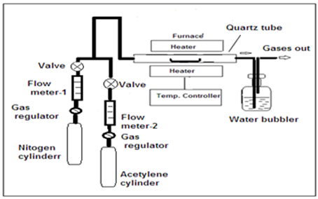
Fig. 1. CVD setup for carbon production.
2.2. Characterization
The morphology of the produced films was investigated using scanning electron microscopy - SEM (Tescan Vega II- Cheek) and transmission electron microscope –TEM (TEM-Philips M10). Powder X-ray diffraction (XRD) of the product was carried out on Shimadzu XRD-6000 X-ray diffractometer equipped with Cu-Kα radiation (λ = 0.154056 nm), employing a scanning speed of 12° min-1 and 2θ ranges from 10° to 60°. Fourier Transform Infrared –FTIR Spectrophotometer (Shimadzu / ARAffinity-1) was used. Raman spectroscopy (Senterra Raman microscope / Germany) was also used for analysing carbon product.
3. Results and Discussion
3.1. XRD Analysis
The crystallinity and graphitization degree of the samples was determined using x- ray diffractometer (XRD). X-Ray powder diffractometric analysis of carbon nanoparticles was carried out to identify their crystal structure. The XRD spectrum of carbon nanoparticles in Fig.2 shows that there are two Bragg diffraction peaks at near 2θ=24.3707º (d=3.64942Ǻ) and 44.0313º (d=2.05490Ǻ) belongs (002) and (101) planes respectively. Where the first peak is smaller than 2θ=26.5º for graphite with an interlayer spacing of d=3.64942Ǻ. It has been reported that the presence of the second peak at 44.01 gives a good indication of the presence of hexagonal graphite lattice [24]. In the present study, the peaks at near 2θ=24.3707º and 44.0313º were indexed as (002) and (101) planes which correspond to the presence of large amounts of amorphous carbon nanomaterial’s in association with hexagonal graphite lattice. These values can also be attributed to the presence of graphene within the carbon sphere product. The broadening of the two peaks suggests the low graphitization degree and the possible presence of amorphous carbon. This outcome is supported by other workers [25].
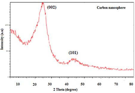
Fig. 2. XRD pattern of carbon nanospheres as synthesized via CVD.
The stacking height (Lc) of the crystallites was calculated in the table (1) using the Scherer’s equation (1) [26].
Lc = 0.89 λ/ β Cos (θ) (1)
Where λ was the wavelength of the radiation used, β was the full width at half maximum (FWHM) of the (002) peak. The average number of carbon atoms (n) per lamellae was calculated which is equal to 3. In this carbon structure, it was found that the calculated crystallite size (Lc) at (002) is a small value 1.16nm. So, the number of carbon atoms (3) as calculated. It was found that the interlayer spacing d002 =3.6494Ǻ increased compared with the graphite due to the small number of carbon atoms. This interplaner spacing (d) value is found to be higher than the values obtained by different coal samples [27]. The XRD data are in a good agreement with other workers results [24]. The high d spacing value was found in agreement with the reported measurements (3.5Å-4.0Å) revealed by TEM only, where these measurements were not confirmed by XRD [28].
Table 1. XRD data for carbon nanosphere and their crystallite size calculations.
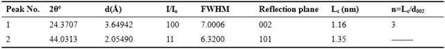
**n is the average number of carbon atoms per lamellae.
3.2. Raman Analysis for CNS's
Figure 3a shows the Raman spectrum of the sample which was analysed using laser source with the wavelength of 532nm. The spectrum presents two peaks centred at 1368.5 and 1594.5 cm−1, which are the typical characteristics of the graphitic carbon nanostructures. The peak at 1594.5 cm−1 (G band) corresponds to an E2g mode of graphite and is related to the vibration of sp2-bonded carbon atoms in a 2-dimensional hexagonal lattice, such as in a graphite layer [29]. The peak at 1368.5 cm−1 (D band) is associated with the vibrations of carbon atoms having dangling bonds in plane terminations of disordered graphite. The first peak is indicating that in the basal plane there exists two-dimensional disorder. Also, the presence of defects in the product is highly possible based on Raman analysis. In general, the relative intensity (ID/IG) ratio is proportional to the number of defects in graphitic carbon. The high ID/IG ratio indicates that some defects are present in the CNPs. It is noted that a wide band instead of sharp peaks and an overlapped D and G band in the region of 1000–2000 cm−1.
Table 2. Raman data for carbon nanosphere and their intensity ratio calculation.
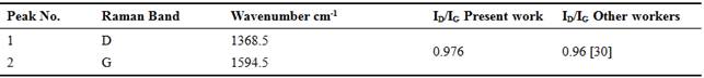
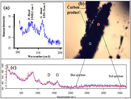
Fig. 3. Raman spectrum (a), images image (b) and its corresponding spectra (c) for the carbon products synthesized via CVD.
3.3. Optical Microscope and SEM Analysis
The prepared carbon materials as deposited on the silicon surface and floated inside the quartz tube without any catalyst are shown in optical microscope photographs of Fig. 4. These materials are also investigated with scanning electron microscope at different magnifications to characterize the surface morphology as shown in Fig. 5. Fig. 5 shows the typical morphology of the synthesized uniform size of spherical particles CNSs from the noncatalytic CVD process. Perfect spherical particle formation generally patterns in spherical particle formation because they possessed lower surface energy. The estimated size of the prepared CNS’s particles is in the range between 100 and 200 nm and most of the particles size about 100 nm as shown in Fig. 6.
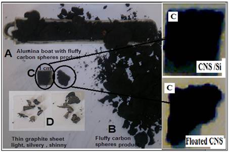
Fig. 4. Optical micrographs of the as prepared CNS's collected from alumina boat (A), quartz tube surface (B), CNs on the silicon substrate and floated CNs(C), and flakes on the quartz tube surface (D).
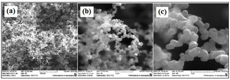
Fig. 5. SEM images with different magnifications of CNS's as synthesized by CVD at 650ºC. (a) Low mag. 1kx, (b) medium mag. 22kx (c) larger mag. 40kx.
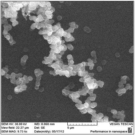
Fig. 6. SEM images of carbon spheres on the silicon substrate, spherical in shape, uniform and their average size ≈ 100 nm.
3.4. Transmission Electron Microscope Analysis
TEM images of the carbon nanospheres are shown in Fig. 7 under different magnifications. It is obviously shown a uniform spherical and solid spheres with diameters in the range of 100-200nm. Solid carbon spheres with forms of beads and necklace –like structures can be seen. These analytical results were confirmed by SEM images.
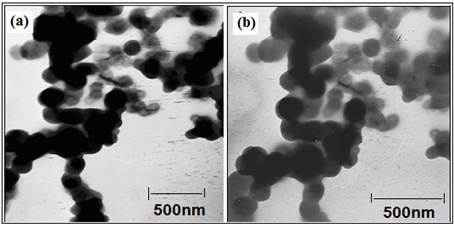
Fig. 7. TEM images of pure CNS as prepared at different magnifications: a) 34000x: b) 43000x.
3.5. Fourier Transforms Infrared Spectroscopy Analysis
The Fourier transform infrared (FTIR) spectrum of the produced carbon is shown in Fig. 8. Small amounts (˂0.5 wt. %) of CNS sample were grounded in potassium bromide (KBr) powder and pressed into a pellet. The absorption bands at 1624.98 cm-1 and 3439.06 cm-1 can be attributed to carbon double bonds C=C and O-H vibrations respectively. There are no other carbon peaks presents in this spectrum, which indicates that high purity product was found.
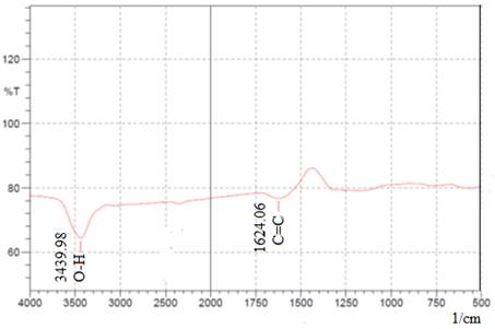
Fig. 8. FTIR spectrum of as-synthesized carbon nanospheres product.
3.6. Optical Properties
The carbon powder was mixed with dimethyl sulphoxide (DMSO) [(CH)3 SO] 99.5% GCC (Supplied by Gainland Chemical Company / UK) and a transparent film on a glass slide were made by drop casting for UV-Vis measurement. The band gap energy was determined using the Tauc’s relation. According to the Tauc’s relation, the absorption coefficient α for direct band gap is given by [31]:
(αhν)2=β(hν−Eg) (2)
Where β is constant, Eg is the optical gap expressed in eV and hν is the photon energy in eV. The direct band gap value Eg is determined by extrapolating the linear part of the (αhν)2 curve towards the hν axis until (αhν)2=0, as shown in Fig. 9. The calculated value of the optical band gap energy Eg is about 3.65 eV for the synthesized CNSs by CVD technique. Our result is higher than the values reported by other workers: Eg=3.5eV [32] and Eg=3.54eV [33].
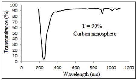
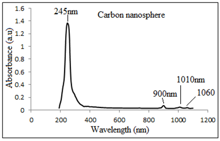
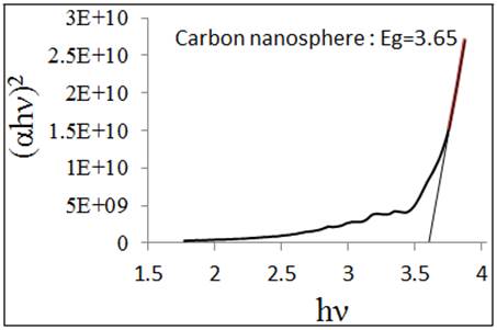
Fig. 9. Tauc’s plot of the synthesized CNS's material by CVD.
4. Conclusions
A large amount of CNS’s was synthesized via chemical vapor deposition process at a moderate reaction temperature. In this paper, author has demonstrated a simple noncatalytic chemical vapor deposition route to produce a lot of carbon nanospheres by direct pyrolysis of the low rate of acetylene gas (~ 7 sccm) as a carbon source mixed with nitrogen as a carrier gas (~93 sccm). The CNS’s were grown on a silicon substrate and fluffy carbon materials were found on the inner surface of the quartz tube. The CNS’s were characterized subsequently by various techniques. The structural quality, surface morphology and optical properties of this product were examined by x-ray diffraction (XRD), Raman spectroscopy, Fourier transform infrared spectroscopy (FTIR), scanning electron microscopy (SEM), transmission electron microscopy (TEM) and Ultraviolet visible spectrophotometer (UV-VIS) respectively. The XRD, Raman and FTIR analysis proved that pure CNS’s are present with amorphous structure. The SEM and TEM confirmed that CNS’s are spherical in shape and having a regular size. On the other hand, the optical properties measurements by UV-VIS for CNS’s are in a good agreement with other data reported elsewhere. High energy gap for carbon product was found, which is mainly interesting results for many applications like sensors, photo-catalysis, and opto-electronic devices.
References
- Yong W., Fabing S., Colin D. W., Jim Y. L., Xiu S. Z.,Ind. Eng. Chem. Res., 47 (7), (2008) 2294–2300.
- Zhenhai W., Qiang W., Qian Z., Jinghong L.,Electrochemistry Communications, 9(8) (2007) 1867–1872.
- Jing W., Zhongbo H., Jianxun X., Yuliang Z., NPG Asia Materials, 6, e84 (2014) 1-12.
- Tie Li, Jianfeng S., Shutong H., Na L., Mingxin Y., Applied Clay Science, 93–94, (2014) 48–55.
- Wojciech K., Krzysztof C., Xuecheng C., Ewa M.,Chemical Engineering Journal, 228, (2013) 824–833.
- Stevens D.A., Dahn JR., Carbon, 43(1) (2005) 179-188.
- Ermete A., Appl. Catal. B: Environtal, 88 (1-2) (2009) 1-24.
- Karolina W., Xuecheng C., Krzysztof K., Jacek M., Ryszard J K., Ewa M., Nanoscale Research Letters, 7, (2012) 269-273.
- Gérrard E. J. P., Sridevi B., MonalibenS., Iafeta L., Derek F., Nanotechnology, Science and Applications, 5, (2012) 49–59.
- Ji B. J., Pil K., Wooyoung K., Jongsik K., Nam D. K., Jongheop Y.,Current Applied Physics, 8 (6) (2008) 814–817.
- Yi Z. J., Chao G., Wen K. H., Yanqiu Z., Andrzej H., Michal B., Martin R., Chi Y. L.,SteveA., Harold K., David R. M. W.,Carbon, 43, (2005) 1944–1953.
- RatchahatS., Viriya-empikul N., Faungnawakij K., Charinpanitkul T., Soottitantawat A., Sci. J. UBU, 1(2) (2010) 40-45.
- ChuyangC., Xudong S., Xuchuan J., Dun N., Aibing Y., ZhigangL.,JiGuang L.,Nanoscale Research Letters, 4, (2009) 971-976.
- Chandra S. S., Manish M. K., Ashutosh S., Marc M.,Chemical Engineering Science, 64, (2009) 1536–1543.
- Chandra S S., Sandip P., Suman S., Ashutosh S., Venkataraghavan R., Bull. Mater. Sci., 32 (3) (2009) 239–246.
- Gilbert D. N., Ahmed A., Haviv G., Erik P., Christopher R. O., Tomer Z., Hart A. J., Doron A., Carl V. T.,Carbon, 50 (11) (2012) 4002–4009.
- Kyotani T, Tsai L., Tomita A.,Chem Mater, 7(8) (1995) 1427–1428.
- Kyotani T, Tsai L., Tomita A.,Chem Mater, 8(8) (1996) 2109–2113.
- Hong-Li Z., Shu-He L., Feng, L., Shuo B, Chang L, Jun T., Hui-Ming C.,Carbon, 44, (2006) 2212–2218.
- OkhyungL., Jaehun J., Seungkyun D., Sung-Soo K., Tae-Hwan N., Kab-Il K.,Yun-Soo L.,Metals and Materials International, 16(4) (2010) 663-667.
- SerpP., Feurer R., Kalck P., Kihn Y, Faria J., Figueiredo J.,Carbon, 39, (2001) 615–628.
- Ugarte D., Nature, 359, (1992)707-709.
- Inagaki M., Carbon, 35 (5), (1997)711-714.
- Mohammad A. H., Shahidul I., American Journal of Nanoscience and Nanotechnology, 1(2) (2013) 52-56.
- Lingjuan D., Gang Z.,Jianfang W., Liping K., Zong-Huai L.,ZupeiY., Zenglin W., Journal of power sources, 196 (24), (2011) 10782-10787.
- Ahmad M., Mohammad R. F., Mohammad R. M., World Journal of Nano Science and Engineering, 2 (2012)154-160.
- Manoj B.,Kunjomana A.G.,Int. J. Electrochem. Sci., 7 (2012) 3127–3134.
- Frusteri, C. Cannilla, K. Barbera, S.Perathoner, G.Centi, F.Frusteri,Carbon 59 (2013)269-307.
- Tuinstra F., Koenig J.L., J.Chem. Phys., 53 (1970) 1126–1130.
- Vivek D., Rao M. V., Prasad J.S., Garima M., Kyong X. R., Hyeon J. K., Dong H. j., Carbon letter, 15 (3)(2014) 198-202.
- Tauc J., Amorphous and liquid semiconductors, Plenum, London, 1974.
- Teo K.B.K,Ferrari A.C. Fanchini G.,Rodil S.E, Yuan Tsai J.J.H.,Laurenti E.,Tagliaferro A., Robertson J., Milne W.J., Diamond and Related Materials 11 (2002) 1086-1090.
- Mani M., Gourav S., Singh K., Pandey O.P.,Journal of Solid State Chemistry 232 (2015)108–117.


