Low Voltage High Performance High Swing Cascode Current Mirror
Umakanta Nanda*, Debasish Nayak
Department of Electronics and Communication Engineering, National Institute of Technology, Rourkela, India
Abstract
A new very high performance low voltage cascode current mirror (CM) circuit is proposed in this work. The CM utilizes the low supply voltage and low input resistance characteristics of a cascode CM. In this CM, cascode configuration is used to obtain a wide operating current range and resistance compensation technique is incorporated to increase the operating bandwidth. The peaking in frequency response is reduced by use of an additional large MOSFET. The proposed CM is simulated by Cadence Analog Design Environment using UMC 90 nm CMOS technology. In the proposed CM a bandwidth of 570 MHz, the 1% settling time of 20 ns, input and output resistances of 25.41 Ω and 770.2 MΩ respectively are obtained with a single supply voltage of 1V.
Keywords
Cascode Current Mirror, Low Supply Voltage, Passive and Active Resistors, Input Output Resistance and Bandwidth
Received: April 10, 2015 / Accepted: April 27, 2015 / Published online: May 15, 2015
@ 2015 The Authors. Published by American Institute of Science. This Open Access article is under the CC BY-NC license. http://creativecommons.org/licenses/by-nc/4.0/
1. Introduction
Increasing trend of using small portable devices has forced the circuit designers with the need of designing circuits operating at low voltages. Trends in IC technology suggest that future implementation of analog/mixed circuits based on standard CMOS technology will operate with power supplies in the range of 1.5V or less [1]. Some techniques like FGMOS have been developed that modify the existing CMOS technology to achieve low supply voltage requirement [2]. A few techniques based on triode/sub-threshold MOSFET operation and bulk-driven MOSFETs were suggested that allow the circuit to operate at low supply voltage without modifying the existing structure of MOSFET [3], [4] . However, these circuits were found to have inherent disadvantages of having low operating range, low bandwidth and low trans-conductance. Recently, flipped voltage follower (FVF) was identified as a basic useful cell, which not only operates at low voltage, but also improves the characteristics of various circuits [5]. In this paper, a new very high performance cascode CM supplied with low voltage is proposed. Cascode version of CM cell has been used to extend the current operating range. Enhancement in bandwidth is achieved by the use of resistance compensation technique in the proposed circuit. To overcome the peaking effect in the frequency response of the CM, an additional large MOSFET is used. This technique significantly improves current transfer accuracy and output resistance of the proposed CM. The paper is organized as follows: high swing cascode CM is explained in section 2. The proposed resistance compensated cascode CM is discussed in section 3. Simulation results of the conventional and the proposed circuit using Cadence Analog Design Environment with UMC 90 nm CMOS technology are shown in section 4, which is followed by the conclusions stated in section 5.
2. High Swing Cascode Current Mirror
As shown in figure 1, a resistor R is used as a voltage divider which creates the bias by dividing the voltage across it [6]. Keeping all the MOSFETs in saturation W/L values of M1 and M3 are calculated using the normal MOSFET drain current formula in saturation.
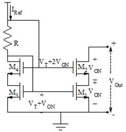
Figure 1. High swing cascode current mirror.
The gates of M2 and M4 are get back biased by VON where substrates of all transistors are grounded. Hence the threshold voltages for M2 and M4 can be calculated [7] as,
![]() (1)
(1)
Hence the gate voltage of M2 and M4 can be calculated as,
![]() (2)
(2)
and gate voltage of M1 and M3 can be found out as,
![]() (3)
(3)
Now, ![]()
The input output characteristics of this high swing cascode current mirror is simulated and shown in figure 2.
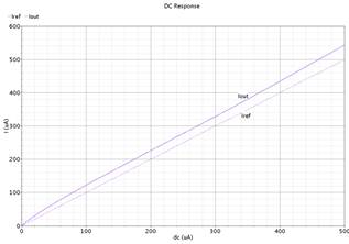
Figure 2. Input output characteristics of high swing cascode current mirror.
3. Modified High Swing Cascode Current Mirror
For bandwidth enhancement designers used a resistor in between the gates of two input and output transistors of the current mirror as shown in figure 3 to introduce a zero in the system. It is called as resistor series peaking.
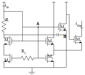
Figure 3. Resistance compensated self bised high swing cascode CM.
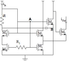
Figure 4. Modified Resistance compensated self bised high swing cascode CM.
But peaking in frequency response is a serious drawback in the CM [8]. To get rid of the peaking effect in the frequency response of the CM, a supplementary large capacitor is introduced. Furthermore, in resister series peaking technique if a higher value of compensating resistance is chosen, then it leads to additional increase in the peaking. This peaking effect is due to gate-source capacitance of M6 which can be reduced by simply incorporating a large capacitor in shunt with it, as shown in figure 4. Since the capacitance is large, it will almost supersede the effect of Cgs of M6. The charging and discharging time of CP does not vary for the entire range of circuit operation, as no current flows through it which overcomes the problem of resistor series peaking caused by Cgs of M6. A choice of large capacitance also reduces the peaking effect caused by resistance compensation leading to increase in bandwidth by large amount without peaking. However, due to negative shunt feedback the total bandwidth of the circuit also gets enhanced.
The nodes A and B in figure 4 are high impedance nodes. The incorporation of the capacitor between these improves the overall stability and phase margin of the circuit.
4. Simulation Results
The CM using the modified technique is simulated in Cadence Specter RF using CMOS 90nm technology with 1V supply. By varying Iin from 0 to 500μA, the DC analysis is carried out. Then the circuit parameters like aspect ratios of the MOSFETs, biasing current and supply voltages are depicted in table 1.
Table 1. Circuit Parameters.
| Component Name | Value |
| M1, M2, M3, M5 | 250nm/90nm |
| M4 | 130nm/90nm |
| M6 | 120nm/90nm |
| M7 | 25μm/90nm |
| VDD | 1 V |
| Iin | 0-500 μA |
In figure 5 the current transfer characteristics has been shown.
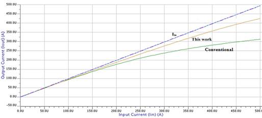
Figure 5. Transfer characteristic of the modified CM.
Here the input current is varied from 0-500 μA. For this range of input current operating in same conditions and with same supply voltage the modified cascode CM raises its current till 425 μA whereas the conventional CM shown in figure 3 has only 312 μA.
Since CM is anticipated for signal path (processing) applications rather than their biasing applications we examined its frequency response which is shown in figure 6 and exhibits relatively high frequency bandwidth of 570 MHz.
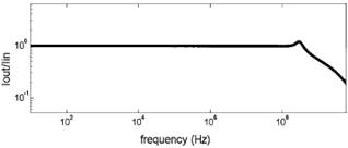
Figure 6. Frequency responce of the modified CM.
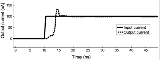
Figure 7. Transient characteristic of the modified CM.
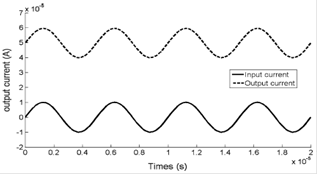
Figure 8. Stability test by inserting a sinusoidal current as input of CM.
The transient response of the modified CM is checked by applying a current step of 100 μA amplitude. The result is shown in figure 7. From this plot it is observed that there is a propagation delay of 5 ns which results due to the extra added R and C in the circuit. Figure 8 shows the output current when applying a sinusoidal current signal in the input node which also proves the stability of the proposed circuit.
5. Conclusion
A modified resistance compensated self bised high swing cascode current mirror is proposed in this work. The circuit is simulated in Cadence Specter RF using CMOS 90nm technology with 1V supply. By varying the input current from 0 to 500 μA it is observed that the output current variation is 25 % more in the proposed technique. From the frequency response curve of the circuit it can be seen that the circuit exhibits relatively high frequency bandwidth of 570 MHz. Moreover this circuit follows the input reference current with a minimized delay of 5 ns where the output current is very much stable as depicted in the stability test. This type of high performance current mirror will be very much handy in the design of various analog and mixed signal circuits in future. However simulation results of component tolerance and process variation can also be included in this work which will shower more robustness on the proposed design.
References
- J Ramirez-Angulo , RG Carvajal , A. Torralba , "Low supply voltage high-performance CMOS current mirror with low input and output voltage requirements," IEEE Transactions on Circuits and Systems II: Express Briefs, vol. 51, pp. 124-129, 2004.
- S Sharma , SS Rajput , LK Magotra , SS Jamuar, "FGMOS based wide range low," in Asia-Pacific Conference on Circuits and Systems, 2002.
- VI Prodanov, MM Green, "CMOS current mirrors with reduced input and output voltage requirements," Electronics letters, vol. 32, pp. 104-105, 1996.
- J Mulder , AC Van Ver Woerd, WA Serdijn , AHM Van Roermund , "High swing cascode MOS current mirror," Electronics letters, vol. 32, pp. 1251-1252, 1996.
- H Chen, KN. Leung, "A Fast-Transient LDO Based on Buffered Flipped Voltage follower," in IEEE International Conference on Electron Devices and Solid-State circuits, China, 2010.
- Philip E Allen, Douglus R Holburg, CMOS Analog Circuit Design, 2nd Edition, Oxford University Press, 2000.
- R. J. Baker, H. W. Li and D. E. Boyce, "CMOS Circuit Design, Layout, and Simulation," IEEE Press Series on Microelectronic Systems, 2002.
- M.-H.Cheng, Z.-W. Wu, "Low-power low-voltage reference using peaking current mirror circuit,"Electronics Letters, vol.41, no.10, pp.572-573, 12 May 2005.


